|
Motore di ricerca datesheet componenti elettronici |
|
|
Motore di ricerca datesheet componenti elettronici |
|
AD9744 Scheda tecnica(PDF) 14 Page - Analog Devices |
|
|
|||||||||||||||||||||||||||||
AD9744 Scheda tecnica(HTML) 14 Page - Analog Devices |
|
|
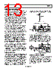
14 / 32 page  AD9744 Rev. B | Page 14 of 32 The control amplifier allows a wide (10:1) adjustment span of IOUTFS over a 2 mA to 20 mA range by setting IREF between 62.5 µA and 625 µA. The wide adjustment span of IOUTFS pro- vides several benefits. The first relates directly to the power dissipation of the AD9744, which is proportional to IOUTFS (refer to the Power Dissipation section). The second relates to the 20 dB adjustment, which is useful for system gain control purposes. The small signal bandwidth of the reference control amplifier is approximately 500 kHz and can be used for low frequency small signal multiplying applications. DAC TRANSFER FUNCTION Both DACs in the AD9744 provide complementary current outputs, IOUTA and IOUTB. IOUTA provides a near full-scale current output, IOUTFS, when all bits are high (that is, DAC CODE = 16383), while IOUTB, the complementary output, provides no current. The current output appearing at IOUTA and IOUTB is a function of both the input code and IOUTFS and can be expressed as ( ) OUTFS I CODE DAC IOUTA × = 16384 / (1) ( ) OUTFS I CODE DAC IOUTB × − = /16384 16383 (2) where DAC CODE = 0 to 16383 (that is, decimal representation). As mentioned previously, IOUTFS is a function of the reference current IREF, which is nominally set by a reference voltage, VREFIO, and external resistor, RSET. It can be expressed as REF OUTFS I I × = 32 (3) where SET REFIO REF R V I / = (4) The two current outputs will typically drive a resistive load di- rectly or via a transformer. If dc coupling is required, IOUTA and IOUTB should be directly connected to matching resistive loads, RLOAD, that are tied to analog common, ACOM. Note that RLOAD may represent the equivalent load resistance seen by IOUTA or IOUTB as would be the case in a doubly terminated 50 Ω or 75 Ω cable. The single-ended voltage output appearing at the IOUTA and IOUTB nodes is simply LOAD OUTA R IOUTA V × = (5) LOAD OUTB R IOUTB V × = (6) Note that the full-scale value of VOUTA and VOUTB should not exceed the specified output compliance range to maintain speci- fied distortion and linearity performance. ( ) LOAD DIFF R IOUTB IOUTA V × − = (7) Substituting the values of IOUTA, IOUTB, IREF, and VDIFF can be expressed as ( ) [ ] () REFIO SET LOAD DIFF V R R CODE DAC V × × − × = / 16384 / 16383 32 2 (8) Equation 7 and Equation 8 highlight some of the advantages of operating the AD9744 differentially. First, the differential operation helps cancel common-mode error sources associated with IOUTA and IOUTB, such as noise, distortion, and dc offsets. Second, the differential code dependent current and subsequent voltage, VDIFF, is twice the value of the single-ended voltage output (that is, VOUTA or VOUTB), thus providing twice the signal power to the load. Note that the gain drift temperature performance for a single- ended (VOUTA and VOUTB) or differential output (VDIFF) of the AD9744 can be enhanced by selecting temperature tracking resistors for RLOAD and RSET due to their ratiometric relationship, as shown in Equation 8. ANALOG OUTPUTS The complementary current outputs in each DAC, IOUTA, and IOUTB may be configured for single-ended or differential operation. IOUTA and IOUTB can be converted into comple- mentary single-ended voltage outputs, VOUTA and VOUTB, via a load resistor, RLOAD, as described in the DAC Transfer Function section by Equation 5 through Equation 8. The differential voltage, VDIFF, existing between VOUTA and VOUTB, can also be converted to a single-ended voltage via a transformer or differential amplifier configuration. The ac performance of the AD9744 is optimum and specified using a differential trans- former-coupled output in which the voltage swing at IOUTA and IOUTB is limited to ±0.5 V. The distortion and noise performance of the AD9744 can be enhanced when it is configured for differential operation. The common-mode error sources of both IOUTA and IOUTB can be significantly reduced by the common-mode rejection of a transformer or differential amplifier. These common-mode error sources include even-order distortion products and noise. The enhancement in distortion performance becomes more significant as the frequency content of the reconstructed wave- form increases and/or its amplitude decreases. This is due to the first-order cancellation of various dynamic common-mode distortion mechanisms, digital feedthrough, and noise. Performing a differential-to-single-ended conversion via a transformer also provides the ability to deliver twice the reconstructed signal power to the load (assuming no source termination). Since the output currents of IOUTA and IOUTB are complementary, they become additive when processed differentially. A properly selected transformer will allow the AD9744 to provide the required power and voltage levels to different loads. |
|
Link URL |
| Lei ha avuto il aiuto da alldatasheet? [ DONATE ] |
Di alldatasheet | Richest di pubblicita | contatti | Privacy Policy | Collegamento alla scheda tecnica | scambio Link | Ricerca produttore All Rights Reserved©Alldatasheet.com |
| Russian : Alldatasheetru.com | Korean : Alldatasheet.co.kr | Spanish : Alldatasheet.es | French : Alldatasheet.fr | Italian : Alldatasheetit.com Portuguese : Alldatasheetpt.com | Polish : Alldatasheet.pl | Vietnamese : Alldatasheet.vn Indian : Alldatasheet.in | Mexican : Alldatasheet.com.mx | British : Alldatasheet.co.uk | New Zealand : Alldatasheet.co.nz |
|
Family Site : ic2ic.com |
icmetro.com |
 Italian ▼
 English
 Chinese
 German
 Japanese
 Russian
 Korean
 Spanish
 French
 Italian
 Portuguese
 Polish
 Vietnamese
 Indian
 Mexican
 British
 New Zealand