|
Motore di ricerca datesheet componenti elettronici |
|
|
Motore di ricerca datesheet componenti elettronici |
|
AD9744 Scheda tecnica(PDF) 16 Page - Analog Devices |
|
|
|||||||||||||||||||||||||||||
AD9744 Scheda tecnica(HTML) 16 Page - Analog Devices |
|
|
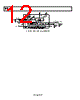
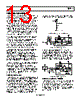
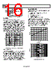
16 / 32 page  AD9744 Rev. B | Page 16 of 32 CLK+ TO DAC CORE CLK– VTT = 1.3V NOM 50 Ω 50 Ω AD9744 CLOCK RECEIVER Figure 29. Clock Termination in PECL Mode DAC TIMING Input Clock and Data Timing Relationship Dynamic performance in a DAC is dependent on the relation- ship between the position of the clock edges and the time at which the input data changes. The AD9744 is rising edge trig- gered, and so exhibits dynamic performance sensitivity when the data transition is close to this edge. In general, the goal when applying the AD9744 is to make the data transition close to the falling clock edge. This becomes more important as the sample rate increases. Figure 30 shows the relationship of SFDR to clock placement with different sample rates. Note that at the lower sample rates, more tolerance is allowed in clock place- ment, while at higher rates, more care must be taken. –3 –2 2 –1 0 1 65 75 ns 3 55 45 35 60 70 50 40 50MHz SFDR 20MHz SFDR 50MHz SFDR Figure 30. SFDR vs. Clock Placement @ fOUT = 20 MHz and 50 MHz Sleep Mode Operation The AD9744 has a power-down function that turns off the out- put current and reduces the supply current to less than 6 mA over the specified supply range of 2.7 V to 3.6 V and tempera- ture range. This mode can be activated by applying a logic level 1 to the SLEEP pin. The SLEEP pin logic threshold is equal to 0.5 Ω AVDD. This digital input also contains an active pull- down circuit that ensures that the AD9744 remains enabled if this input is left disconnected. The AD9744 takes less than 50 ns to power down and approximately 5 µs to power back up. POWER DISSIPATION The power dissipation, PD, of the AD9744 is dependent on sev- eral factors that include: • The power supply voltages (AVDD, CLKVDD, and DVDD) • The full-scale current output IOUTFS • The update rate fCLOCK • The reconstructed digital input waveform The power dissipation is directly proportional to the analog supply current, IAVDD, and the digital supply current, IDVDD. IAVDD is directly proportional to IOUTFS, as shown in Figure 31, and is insensitive to fCLOCK. Conversely, IDVDD is dependent on both the digital input waveform, fCLOCK, and digital supply DVDD. Figure 32 shows IDVDD as a function of full-scale sine wave output ratios (fOUT/fCLOCK) for various update rates with DVDD = 3.3 V. IOUTFS (mA) 35 0 2 30 25 20 15 10 4 6 8 101214 161820 Figure 31. IAVDD vs. IOUTFS RATIO (fOUT/fCLOCK) 20 0.01 1 0.1 14 16 18 12 10 8 6 4 2 0 165MSPS 210MSPS 65MSPS 125MSPS Figure 32. IDVDD vs. Ratio @ DVDD = 3.3 V |
|
Link URL |
| Lei ha avuto il aiuto da alldatasheet? [ DONATE ] |
Di alldatasheet | Richest di pubblicita | contatti | Privacy Policy | Collegamento alla scheda tecnica | scambio Link | Ricerca produttore All Rights Reserved©Alldatasheet.com |
| Russian : Alldatasheetru.com | Korean : Alldatasheet.co.kr | Spanish : Alldatasheet.es | French : Alldatasheet.fr | Italian : Alldatasheetit.com Portuguese : Alldatasheetpt.com | Polish : Alldatasheet.pl | Vietnamese : Alldatasheet.vn Indian : Alldatasheet.in | Mexican : Alldatasheet.com.mx | British : Alldatasheet.co.uk | New Zealand : Alldatasheet.co.nz |
|
Family Site : ic2ic.com |
icmetro.com |
 Italian ▼
 English
 Chinese
 German
 Japanese
 Russian
 Korean
 Spanish
 French
 Italian
 Portuguese
 Polish
 Vietnamese
 Indian
 Mexican
 British
 New Zealand