 |
Motore di ricerca datesheet componenti elettronici |
|
|
Motore di ricerca datesheet componenti elettronici |
|
The question interval is too short.
Please try again in a few seconds.

Hello, Please ask a question about AD7303 Datasheet
# Example questions:
➢ Figure 10 shows settling time. what is being measured when observing the settling time and what seems to be happening during that time?
➢ What is the approximate output source current capability of the device when vdd is 3v?
➢ What are the two main options for the reference voltage used by this device?
| Part No. | AD7303 |
| Manufacturer | AD |
| Size | 361 Kbytes |
| Pages | 16 pages |
| Description | +2.7 V to +5.5 V, Serial Input, Dual Voltage Output 8-Bit DAC |







1. Device Overview & Intended Use:
️· This is a DAC, likely part of a larger system.
️· The diagrams suggest it's designed for applications requiring some degree of precision and speed (settling time).
️· Power-down features are included (Figure 11), indicating a focus on power efficiency.
2. Key Specifications (Based on Text & Diagrams - Note that some values are *estimates* based on the figures):
️· Power Supply: It operates with both 3V and 5V power supplies. Figure 3 and 5 show source current vs. voltage.
️· Reference Voltage: Figure 6 shows Relative Accuracy vs External Reference voltage, suggesting an external reference is used. A value of approximately 2.6V for the external reference achieves decent accuracy.
️· Settling Time: Figure 10 displays settling time. The text indicates a settling time of less than 200ns for a full scale change.
️· Frequency Response: Figure 9 illustrates the frequency response. There is still significant amplitude remaining at 10 kHz.
️· Accuracy & Error: Figure 7 depicts Relative Accuracy vs. External Reference Voltage. Relative Accuracy stays high until the external reference is reduced. Figure 6 also displays INL (Integral Non-Linearity) and DNL (Differential Non-Linearity) errors, although specific values are difficult to read precisely from the diagrams.
3. Features:
️· Power-Down Mode: Allows for low-power operation. Figure 11 shows the power-down exit time.
️· External Reference: Uses an external reference voltage for improved accuracy and flexibility.
️· Multiple Power Supply Options: Flexibility in power supply choices.
️· Analog Output: Provides a continuous analog voltage output.
️· Synchronization: Figure 5, illustrates synchronization features.
4. Diagram Interpretation:
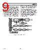
️· Figure 1 & 2: Likely block diagrams showing the DAC's architecture (not fully discernible from text).
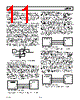
️· Figure 11 (Power-Down): Shows the power-down exit time, indicating how quickly the DAC returns to normal operation after exiting power-down mode.
️· Figure 6 (Relative Accuracy): Illustrates the impact of external reference voltage on the DAC's accuracy.
️· Figure 10 (Settling Time): Shows settling time for a full-scale change in the output voltage, an important performance metric.
️· Figures 3, 5, 3: Shows source current versus voltage/temperature.
5. Things That Need More Information To Understand Fully:
️· Specific DAC Architecture: The block diagrams are not detailed enough to understand the internal architecture fully.
️· Resolution and Step Size: The text doesn’t specify the DAC's resolution (number of bits) or the resulting step size.
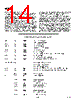
️· Input Data Format: The format of the digital input data (e.g., parallel, serial, SPI, I2C) is not described.
️· Specific Error Values: The exact numerical values for INL and DNL are difficult to determine from the diagrams.
Important Disclaimer: This summary is based solely on the provided text and diagrams. For complete and accurate information, please refer to the full datasheet or technical documentation for the DAC.
1. Device Overview & Intended Use:
️· This is a DAC, likely part of a larger system.
️· The diagrams suggest it's designed for applications requiring some degree of precision and speed (settling time).
️· Power-down features are included (Figure 11), indicating a focus on power efficiency.
2. Key Specifications (Based on Text & Diagrams - Note that some values are *estimates* based on the figures):
️· Power Supply: It operates with both 3V and 5V power supplies. Figure 3 and 5 show source current vs. voltage.
️· Reference Voltage: Figure 6 shows Relative Accuracy vs External Reference voltage, suggesting an external reference is used. A value of approximately 2.6V for the external reference achieves decent accuracy.
️· Settling Time: Figure 10 displays settling time. The text indicates a settling time of less than 200ns for a full scale change.
️· Frequency Response: Figure 9 illustrates the frequency response. There is still significant amplitude remaining at 10 kHz.
️· Accuracy & Error: Figure 7 depicts Relative Accuracy vs. External Reference Voltage. Relative Accuracy stays high until the external reference is reduced. Figure 6 also displays INL (Integral Non-Linearity) and DNL (Differential Non-Linearity) errors, although specific values are difficult to read precisely from the diagrams.
3. Features:
️· Power-Down Mode: Allows for low-power operation. Figure 11 shows the power-down exit time.
️· External Reference: Uses an external reference voltage for improved accuracy and flexibility.
️· Multiple Power Supply Options: Flexibility in power supply choices.
️· Analog Output: Provides a continuous analog voltage output.
️· Synchronization: Figure 5, illustrates synchronization features.
4. Diagram Interpretation:
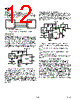
️· Figure 1 & 2: Likely block diagrams showing the DAC's architecture (not fully discernible from text).
️· Figure 11 (Power-Down): Shows the power-down exit time, indicating how quickly the DAC returns to normal operation after exiting power-down mode.
️· Figure 6 (Relative Accuracy): Illustrates the impact of external reference voltage on the DAC's accuracy.
️· Figure 10 (Settling Time): Shows settling time for a full-scale change in the output voltage, an important performance metric.
️· Figures 3, 5, 3: Shows source current versus voltage/temperature.
5. Things That Need More Information To Understand Fully:
️· Specific DAC Architecture: The block diagrams are not detailed enough to understand the internal architecture fully.
️· Resolution and Step Size: The text doesn’t specify the DAC's resolution (number of bits) or the resulting step size.
️· Input Data Format: The format of the digital input data (e.g., parallel, serial, SPI, I2C) is not described.
️· Specific Error Values: The exact numerical values for INL and DNL are difficult to determine from the diagrams.
Important Disclaimer: This summary is based solely on the provided text and diagrams. For complete and accurate information, please refer to the full datasheet or technical documentation for the DAC.
| Part No. | AD7303 |
| Manufacturer | AD |
| Size | 361 Kbytes |
| Pages | 16 pages |
| Description | +2.7 V to +5.5 V, Serial Input, Dual Voltage Output 8-Bit DAC |
| Lei ha avuto il aiuto da alldatasheet? [ DONATE ] |
Di alldatasheet | Richest di pubblicita | contatti | Privacy Policy | Collegamento alla scheda tecnica | scambio Link | Ricerca produttore All Rights Reserved©Alldatasheet.com |
| Russian : Alldatasheetru.com | Korean : Alldatasheet.co.kr | Spanish : Alldatasheet.es | French : Alldatasheet.fr | Italian : Alldatasheetit.com Portuguese : Alldatasheetpt.com | Polish : Alldatasheet.pl | Vietnamese : Alldatasheet.vn Indian : Alldatasheet.in | Mexican : Alldatasheet.com.mx | British : Alldatasheet.co.uk | New Zealand : Alldatasheet.co.nz |
|
Family Site : ic2ic.com |
icmetro.com |
 Italian ▼
  English
 Chinese
 German
 Japanese
 Russian
 Korean
 Spanish
 French
 Portuguese
 Polish
 Vietnamese
 Indian
 Mexican
 British
 New Zealand