|
Motore di ricerca datesheet componenti elettronici |
|
|
Motore di ricerca datesheet componenti elettronici |
|
AD7303 Scheda tecnica(PDF) 13 Page - Analog Devices |
|
|
|||||||||||||||||||||||||||||
AD7303 Scheda tecnica(HTML) 13 Page - Analog Devices |
|
|
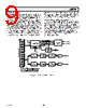
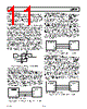
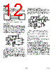
13 / 16 page  AD7303 –13– REV. 0 SCLK VDD 10k Ω AD7303 DIN SYNC SCLK VDD REF POWER +5V REGULATOR VOUTB VOUTA AGND 10µF 0.1µF 0.1µF VDD 10k Ω DATA VDD 10k Ω SYNC Figure 32. AD7303 in Opto-Isolated Interface Decoding Multiple AD7303 The SYNC pin on the AD7303 can be used in applications to decode a number of DACs. In this application, all DACs in the system receive the same serial clock and serial data, but only the SYNC to one of the DACs will be active at any one time allow- ing access to two channels in this eight-channel system. The 74HC139 is used as a 2- to 4-line decoder to address any of the DACs in the system. To prevent timing errors from occurring, the enable input should be brought to its inactive state while the coded address inputs are changing state. Figure 33 shows a dia- gram of a typical setup for decoding multiple AD7303 devices in a system. ENABLE 74HC139 AD7303 SYNC DIN SCLK DIN SCLK DGND CODED ADDRESS 1A 1B 1Y0 1Y1 1Y2 1Y3 VCC VDD 1 G AD7303 SYNC DIN SCLK AD7303 SYNC DIN SCLK AD7303 SYNC DIN SCLK Figure 33. Decoding Multiple AD7303 Devices in a System AD7303 as a Digitally Programmable Window Detector A digitally programmable upper/lower limit detector using the two DACs in the AD7303 is shown in Figure 34. The upper and lower limits for the test are loaded to DACs A and B which, in turn, set the limits on the CMP04. If a signal at the VIN input is not within the programmed window, a led will indicate the fail condition. AD7303 VDD +5V VOUTA GND 0.1µF REF VIN PASS/ FAIL 1/2 CMP04 1/6 74HC05 FAIL PASS 1k Ω 0.1µF 10µF SCLK DIN SYNC SCLK DIN SYNC 1k Ω VOUTB Figure 34. Window Detector Using AD7303 Programmable Current Source Figure 35 shows the AD7303 used as the control element of a programmable current source. In this circuit, the full-scale cur- rent is set to 1 mA. The output voltage from the DAC is applied across the current setting resistor of 4.7 k Ω in series with the full-scale setting resistor of 470 Ω. Suitable transistors to place in the feedback loop of the amplifier include the BC107 and the 2N3904, which enable the current source to operate from a min VSOURCE of 6 V. The operating range is determined by the oper- ating characteristics of the transistor. Suitable amplifiers in- clude the AD820 and the OP295, both having rail-to-rail operation on their outputs. The current for any digital input code can be calculated as follows: I = 2 × V REF × D/(5E + 3 × 256) mA 4.7k Ω 470 Ω +5V LOAD VSOURCE AD7303 VOUTA 10µF 0.1µF VDD = +5V VDD GND AD780/ REF192 WITH VDD = +5V REF SCLK DIN SYNC GND VOUT VIN 0.1µF SERIAL INTERFACE EXT REF AD820/ OP295 Figure 35. Programmable Current Source |
|
|
Link URL |
| Lei ha avuto il aiuto da alldatasheet? [ DONATE ] |
Di alldatasheet | Richest di pubblicita | contatti | Privacy Policy | Collegamento alla scheda tecnica | scambio Link | Ricerca produttore All Rights Reserved©Alldatasheet.com |
| Russian : Alldatasheetru.com | Korean : Alldatasheet.co.kr | Spanish : Alldatasheet.es | French : Alldatasheet.fr | Italian : Alldatasheetit.com Portuguese : Alldatasheetpt.com | Polish : Alldatasheet.pl | Vietnamese : Alldatasheet.vn Indian : Alldatasheet.in | Mexican : Alldatasheet.com.mx | British : Alldatasheet.co.uk | New Zealand : Alldatasheet.co.nz |
|
Family Site : ic2ic.com |
icmetro.com |
 Italian ▼
 English
 Chinese
 German
 Japanese
 Russian
 Korean
 Spanish
 French
 Italian
 Portuguese
 Polish
 Vietnamese
 Indian
 Mexican
 British
 New Zealand