|
Motore di ricerca datesheet componenti elettronici |
|
|
Motore di ricerca datesheet componenti elettronici |
|
AD7303 Scheda tecnica(PDF) 14 Page - Analog Devices |
|
|
|||||||||||||||||||||||||||||
AD7303 Scheda tecnica(HTML) 14 Page - Analog Devices |
|
|
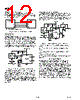
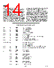
14 / 16 page  AD7303 –14– REV. 0 AD7303 to 68HC11 Interface Program Source Code * PORTC EQU $1003 Port C Control Register * "SYNC, 0, 0, 0, 0, 0, 0, 0" DDRC EQU $1007 Port C Data Direction PORTD EQU $1008 Port D Data Register * "0, 0, 0, SCLK, DIN, 0, 0, 0" DDRD EQU $1009 Port D Data Direction SPCR EQU $1028 SPI Control Register * "SPIE, SPE, DWOM, MSTR, CPOL, CPHA, SPR1, SPR0" SPSR EQU $1029 SPI Status Register * "SPIF, WCOL, 0, MODF, 0, 0, 0, 0" SPDR EQU $102A SPI Data Register, Read Buffer, Write Shifter * * SDI RAM Variables: DIN 1 is eight MSBs, Control BYTE DIN 2 is eight LSBs, Data BYTE DAC requires 2*8-bit Writes DIN1 EQU $00 DIN BYTE 1: " INT/EXT, X, LDAC, PDB, PBA, A/B, CR1, CR0" DIN2 EQU $01 DIN BYTE 2: " DB7, DB6, DB5, DB4, DB3, DB2, DB1, DB0" * ORG $C000 Start of users ram INIT LDS #$CFFF Top of C page Ram * LDAA #$80 1, 0, 0, 0, 0, 0, 0, 0 * SYNC is High STAA PORTC Initialize Port C Outputs LDAA #$80 1, 0, 0, 0, 0, 0, 0, 0 STAA DDRC SYNC enabled as output * LDAA #$00 0, 0, 0, 0, 0, 0, 0, 0 * SCLK is low, DIN is low STAA PORTD Initialize Port D outputs Power Supply Bypassing and Grounding In any circuit where accuracy is important, careful consideration of the power supply and ground return layout helps to ensure the rated performance. The printed circuit board on which the AD7303 is mounted should be designed so that the analog and digital sections are separated, and confined to certain areas of the board. If the AD7303 is in a system where multiple devices require an AGND to DGND connection, the connec- tion should be made at one point only. The star ground point should be established as closely as possible to the AD7303. The AD7303 should have ample supply bypassing of 10 µF in paral- lel with 0.1 µF on the supply located as closely to the package as possible, ideally right up against the device. The 10 µF capaci- tors are the tantalum bead type. The 0.1 µF capacitor should have low Effective Series Resistance (ESR) and Effective Series Inductance (ESI), like the common ceramic types that provide a low impedance path to ground at high frequencies to handle transient currents due to internal logic switching. The power supply lines of the AD7303 should use as large a trace as possible to provide low impedance paths and reduce the effects of glitches on the power supply line. Fast switching sig- nals such as clocks should be shielded with digital ground to avoid radiating noise to other parts of the board, and should never be run near the reference inputs. Avoid crossover of digi- tal and analog signals. Traces on opposite sides of the board should run at right angles to each other. This reduces the effects of feedthrough through the board. A microstrip technique is by far the best, but not always possible with a double-sided board. In this technique, the component side of the board is dedicated to ground plane while signal traces are placed on the solder side. |
|
|
Link URL |
| Lei ha avuto il aiuto da alldatasheet? [ DONATE ] |
Di alldatasheet | Richest di pubblicita | contatti | Privacy Policy | Collegamento alla scheda tecnica | scambio Link | Ricerca produttore All Rights Reserved©Alldatasheet.com |
| Russian : Alldatasheetru.com | Korean : Alldatasheet.co.kr | Spanish : Alldatasheet.es | French : Alldatasheet.fr | Italian : Alldatasheetit.com Portuguese : Alldatasheetpt.com | Polish : Alldatasheet.pl | Vietnamese : Alldatasheet.vn Indian : Alldatasheet.in | Mexican : Alldatasheet.com.mx | British : Alldatasheet.co.uk | New Zealand : Alldatasheet.co.nz |
|
Family Site : ic2ic.com |
icmetro.com |
 Italian ▼
 English
 Chinese
 German
 Japanese
 Russian
 Korean
 Spanish
 French
 Italian
 Portuguese
 Polish
 Vietnamese
 Indian
 Mexican
 British
 New Zealand