|
Motore di ricerca datesheet componenti elettronici |
|
|
Motore di ricerca datesheet componenti elettronici |
|
EP9315 Scheda tecnica(PDF) 6 Page - Cirrus Logic |
|
|
|||||||||||||||||||||||||||||
EP9315 Scheda tecnica(HTML) 6 Page - Cirrus Logic |
|
|
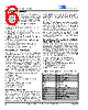
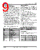
6 / 64 page  6 ©Copyright 2005 Cirrus Logic (All Rights Reserved) DS638PP4 EP9315 Enhanced Universal Platform SOC Processor Processor Core - ARM920T The ARM920T is a Harvard architecture processor with separate 16-kbyte instruction and data caches with an 8- word line length but a unified memory. The processor utilizes a five-stage pipeline consisting of fetch, decode, execute, memory, and write stages. Key features include: • ARM (32-bit) and Thumb (16-bit compressed) Instruction Sets • 32-bit Advanced Micro-Controller Bus Architecture (AMBA) • 16-kbyte Instruction Cache with Lockdown • 16-kbyte Data Cache (programmable write-through or write-back) with Lockdown • MMU for Linux®, Microsoft® Windows® CE and Other Operating Systems • Translation Look Aside Buffers with 64 Data and 64 Instruction Entries • Programmable Page Sizes of 1 Mbyte, 64 kbyte, 4 kbyte, and 1 kbyte • Independent Lockdown of TLB Entries MaverickCrunch™ Math Engine The MaverickCrunch Engine is a mixed-mode coprocessor designed primarily to accelerate the math processing required to rapidly encode digital audio formats. It accelerates single and double precision integer and floating point operations plus an integer multiply-accumulate (MAC) instruction that is considerably faster than the ARM920T's native MAC instruction. The ARM920T coprocessor interface is utilized thereby sharing its memory interface and instruction stream. Hardware forwarding and interlock allows the ARM to handle looping and addressing while MaverickCrunch handles computation. Features include: • IEEE-754 single and double precision floating point • 32 / 64-bit integer • Add / multiply / compare • Integer MAC 32-bit input with 72-bit accumulate • Integer Shifts • Floating point to/from integer conversion • Sixteen 64-bit register files • Four 72-bit accumulators MaverickKey™ Unique ID MaverickKey unique hardware programmed IDs are a solution to the growing concern over secure web content and commerce. With Internet security playing an important role in the delivery of digital media such as books or music, traditional software methods are quickly becoming unreliable. The MaverickKey unique IDs provide OEMs with a method of utilizing specific hardware IDs such as those assigned for SDMI (Secure Digital Music Initiative) or any other authentication mechanism. Both a specific 32-bit ID as well as a 128-bit random ID is programmed into the EP9315 through the use of laser probing technology. These IDs can then be used to match secure copyrighted content with the ID of the target device the EP9315 is powering, and then deliver the copyrighted information over a secure connection. In addition, secure transactions can benefit by also matching device IDs to server IDs. MaverickKey IDs provide a level of hardware security required for today’s Internet appliances. General Purpose Memory Interface (SDRAM, SRAM, ROM, FLASH) The EP9315 features a unified memory address model where all memory devices are accessed over a common address/data bus. A separate internal port is dedicated to the read-only Raster/LCD refresh engine, while the rest of the memory accesses are performed via the Processor bus. The SRAM memory controller supports 8, 16 and 32-bit devices and accommodates an internal boot ROM concurrently with 32-bit SDRAM memory. • 1-4 banks of 32-bit 66 or 100 MHz SDRAM • One internal port dedicated to the Raster/LCD Refresh Engine (Read Only) • Address and data bus shared between SDRAM, SRAM, ROM, and FLASH memory • NOR FLASH memory supported Table B. General Purpose Memory Interface Pin Assignments Pin Mnemonic Pin Description SDCLK SDRAM Clock SDCLKEN SDRAM Clock Enable SDCSn[3:0] SDRAM Chip Selects 3-0 RASn SDRAM RAS CASn SDRAM CAS SDWEn SDRAM Write Enable CSn[7:6] and CSn[3:0] Chip Selects 7, 6, 3, 2, 1, 0 AD[25:0] Address Bus 25-0 DA[31:0] Data Bus 31-0 DQMn[3:0] SDRAM Output Enables / Data Masks WRn SRAM Write Strobe RDn SRAM Read / OE Strobe WAITn SRAM Wait Input |
|
Link URL |
| Lei ha avuto il aiuto da alldatasheet? [ DONATE ] |
Di alldatasheet | Richest di pubblicita | contatti | Privacy Policy | Collegamento alla scheda tecnica | scambio Link | Ricerca produttore All Rights Reserved©Alldatasheet.com |
| Russian : Alldatasheetru.com | Korean : Alldatasheet.co.kr | Spanish : Alldatasheet.es | French : Alldatasheet.fr | Italian : Alldatasheetit.com Portuguese : Alldatasheetpt.com | Polish : Alldatasheet.pl | Vietnamese : Alldatasheet.vn Indian : Alldatasheet.in | Mexican : Alldatasheet.com.mx | British : Alldatasheet.co.uk | New Zealand : Alldatasheet.co.nz |
|
Family Site : ic2ic.com |
icmetro.com |
 Italian ▼
 English
 Chinese
 German
 Japanese
 Russian
 Korean
 Spanish
 French
 Italian
 Portuguese
 Polish
 Vietnamese
 Indian
 Mexican
 British
 New Zealand