|
Motore di ricerca datesheet componenti elettronici |
|
|
Motore di ricerca datesheet componenti elettronici |
|
STEC01 Scheda tecnica(PDF) 3 Page - STMicroelectronics |
|
|
|||||||||||||||||||||||||||||
STEC01 Scheda tecnica(HTML) 3 Page - STMicroelectronics |
|
|
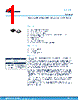
3 / 22 page  2 Pin configuration Figure 2. Pin configuration Table 1. Pin configuration Symbol Pin Description RESET\FAULT 1 Open drain output, active low. It generates a 57 ms pulse if a fault condition is detected or when HW_RESET\USB is pulled high VBAT 2 Battery supply voltage. Bypass this pin to GND with a 1 µF ceramic capacitor AGND 3 Analog GND. Connect it to a dedicated ground path TPF 4 T1 oscillator programming pin. Connect a resistor to GND, to achieve a frequency ranging from 100 kHz to 400 kHz T1P1 5 T1 timer programming pin. Connect to VBAT, GND or floating to select T1 prescaler (hard wired). See Figure 5. Timer configuration truth table T1P2 6 T3P 7 T3 timer programming pin. Connect to VBAT, GND or floating (hard wired). See Figure 5. Timer configuration truth table PGND 8, 9, 10 Power ground (internal N-channel power MOS source terminal) PWR 11, 12, 13 Input power voltage (internal N-channel power MOS drain terminal) GDRV 14 Gate driver output. Leave floating if it is not used HW_RESET\USB 15 Input hardware reset. Do not leave floating. If it is not used, put to GND PWM 16 Input control signal, 4 Hz to 5 kHz, 30%-100% duty cycle GND EXP Exposed pad, connect to thermal ground plane STEC01 Pin configuration DS13063 - Rev 2 page 3/22 |
|
|
Link URL |
| Lei ha avuto il aiuto da alldatasheet? [ DONATE ] |
Di alldatasheet | Richest di pubblicita | contatti | Privacy Policy | Collegamento alla scheda tecnica | scambio Link | Ricerca produttore All Rights Reserved©Alldatasheet.com |
| Russian : Alldatasheetru.com | Korean : Alldatasheet.co.kr | Spanish : Alldatasheet.es | French : Alldatasheet.fr | Italian : Alldatasheetit.com Portuguese : Alldatasheetpt.com | Polish : Alldatasheet.pl | Vietnamese : Alldatasheet.vn Indian : Alldatasheet.in | Mexican : Alldatasheet.com.mx | British : Alldatasheet.co.uk | New Zealand : Alldatasheet.co.nz |
|
Family Site : ic2ic.com |
icmetro.com |
 Italian ▼
 English
 Chinese
 German
 Japanese
 Russian
 Korean
 Spanish
 French
 Italian
 Portuguese
 Polish
 Vietnamese
 Indian
 Mexican
 British
 New Zealand