|
Motore di ricerca datesheet componenti elettronici |
|
|
Motore di ricerca datesheet componenti elettronici |
|
L9961-TR Scheda tecnica(PDF) 17 Page - STMicroelectronics |
|
|
|||||||||||||||||||||||||||||
L9961-TR Scheda tecnica(HTML) 17 Page - STMicroelectronics |
|
|
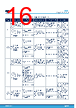
17 / 65 page  Fault type Assertion condition IC reaction to assertion Release condition IC reaction to flag clear Maskable Cell severe OV If a cell voltage raises above VCELL_SEVERE_OV_ TH, the severe OV fault is acknowledged FUSE pre-driver is enabled If a cell voltage falls below VCELL_SEVERE_OV_ TH, the cell severe OV flag can be cleared by MCU FAULTN line is released CELL_SEVERE_OV_F USE_MSK masks reaction on FUSE pin FAULTN_SAFE is pulled low for TFAULTN_SAFE_LOW (if a pulse on FAULTN_SAFE pin was not already generated after a previous not masked and not cleared Cell OV / Cell Severe OV detection) CELL_SEVERE_OV_R ST_MSK masks reaction FAULTN_SAFE pin FAULTN line is asserted CELL_SEVERE_OV_FA ULTN_MSK masks reaction on FAULTN pin Cell balance UV If a cell voltage falls below VCELL_BAL_UV_TH, the corresponding Bal UV counter is incremented by 1 The BAL<x>_UV flag is set If a cell voltage raises above VCELL_BAL_UV_TH, the corresponding Bal UV counter is decremented by 1. The Balancing FET is restored to the status defined by the corresponding BAL<x>_ON bit VCELL<x>_EN masks measurement execution. The Bal UV flag of a disabled cell can always be cleared If the Bal UV counter reaches VCELL_BAL_UV_CNT_ TH, it saturates the Bal UV fault is acknowledged Any ongoing balancing is stopped on the affected cell, regardless of BAL<x>_ON bit If the Bal UV counter reaches zero, the Bal UV flag can be cleared by MCU FAULTN line is released BAL_UV_BAL_MSK masks reaction on balancing FAULTN line is asserted BAL_UV_FAULTN_MSK masks reaction on FAULTN pin 3.4.1.1 Electrical parameters All parameters are tested and guaranteed in the following conditions, unless otherwise noted: VB according to the operating range of Table 2; TJ according to the operating range of Table 5. Table 11. Cell voltage monitor electrical parameters Symbol Parameter Test conditions Min. Typ. Max. Unit VCELL_RANGE Cell voltage input measurement range Design info 1 4.7 V VCELL_RES Cell voltage measurement resolution Design info, effective range [0-5]V 1.22 (5 V/212) mV NBIT ADC bit number Design info 12 bit ICELL_LEAK Cx leakage current ADC not converting 500 nA VCELLERR1 ADC total conversion error range 1 1 V ≤ VCELL < 1.5 V -40 °C< TJ<120 °C -25 25 mV VCELLERR2 ADC total conversion error range 2 1.5 V ≤ VCELL ≤ 4.5 V -40 °C< TJ<105 °C -15 15 mV VCELLERR3 ADC total conversion error range 3 4.5 V ≤ VCELL ≤ 4.7 V -40 °C< TJ<120°C -25 25 mV VCELLERR4 ADC total conversion error range 4 1.5 V ≤ VCELL ≤ 4.5 V -25 25 mV L9961 Voltage conversion routine DS14012 - Rev 3 page 17/65 |
|
Link URL |
| Lei ha avuto il aiuto da alldatasheet? [ DONATE ] |
Di alldatasheet | Richest di pubblicita | contatti | Privacy Policy | Collegamento alla scheda tecnica | scambio Link | Ricerca produttore All Rights Reserved©Alldatasheet.com |
| Russian : Alldatasheetru.com | Korean : Alldatasheet.co.kr | Spanish : Alldatasheet.es | French : Alldatasheet.fr | Italian : Alldatasheetit.com Portuguese : Alldatasheetpt.com | Polish : Alldatasheet.pl | Vietnamese : Alldatasheet.vn Indian : Alldatasheet.in | Mexican : Alldatasheet.com.mx | British : Alldatasheet.co.uk | New Zealand : Alldatasheet.co.nz |
|
Family Site : ic2ic.com |
icmetro.com |
 Italian ▼
 English
 Chinese
 German
 Japanese
 Russian
 Korean
 Spanish
 French
 Italian
 Portuguese
 Polish
 Vietnamese
 Indian
 Mexican
 British
 New Zealand