|
Motore di ricerca datesheet componenti elettronici |
|
|
Motore di ricerca datesheet componenti elettronici |
|
RC19302A00AGNT#KD0 Scheda tecnica(PDF) 7 Page - Renesas Technology Corp |
|
|
|||||||||||||||||||||||||||||
RC19302A00AGNT#KD0 Scheda tecnica(HTML) 7 Page - Renesas Technology Corp |
|
|
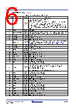
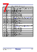
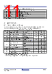
7 / 62 page  R31DS0210EU0106 Rev.1.06 Page 7 May 11, 2026 RC193xx Datasheet 29 LOSb O, OD, PDT Output indicating Loss of Input Signal. This pin is an open drain output and requires an external pull up resistor for proper functionality. A low output on this pin indicates a loss of signal on the input clock. 30 VDDCLK_0 PWR Power supply for clock output bank 0. 31 VDDA PWR Power supply for core multiplexer circuitry. 32 CLK3 O, DIF True clock output. 33 CLKb3 O, DIF Complementary clock output. 34 OEb3 I, SE, PU, PDT Active low input for enabling output 3. 0 = Enable output, 1 = Disable output. 35 OEb2 I, SE, PU, PDT Active low input for enabling output 2. 0 = Enable output, 1 = Disable output. 36 SADR_tri1 I, SE, PD, PU SMBus address bit. This is a tri-level input that works in conjunction with other SADR pins, if present, to decode SMBus Addresses. See the SMBus Address Selection (RC19308) table and refer to the tri-level input thresholds in the electrical tables. 37 CLK2 O, DIF True clock output. 38 CLKb2 O, DIF Complementary clock output. 39 VDDCLK_0 PWR Power supply for clock output bank 0. 40 CLK1 O, DIF True clock output. 41 CLKb1 O, DIF Complementary clock output. 42 (RC19308A) SLEWRATE_SEL I, SE, PU, PDT Input to select default output slew rate. 0 = Slow slew rate. 1 = Fast slew rate. 42 (RC19308A0 01) AMPLITUDE_SEL I, SE, PD, PDT Input to select output amplitude. The values are programmable with defaults listed below. See AMP_CTRL_DEF for default amplitude and AMP_CTRL_ALT for alternate amplitude. 0 = Select Default Amplitude (800mV), 1 = Select Alternate Amplitude (900mV) 43 OEb1 I, SE, PU, PDT Active low input for enabling output 1. 0 = Enable output, 1 = Disable output. 44 OEb0 I, SE, PU, PDT Active low input for enabling output 0. 0 = Enable output, 1 = Disable output. 45 CLK0 O, DIF True clock output. 46 CLKb0 O, DIF Complementary clock output. 47 VDDCLK_0 PWR Power supply for clock output bank 0. 48 GNDSUB GND Ground pin for substrate. 49 EPAD PWR Ground. Table 1. RC19308A/A001 Pin Descriptions (Cont.) Pin Number Pin Name Type Description |
|
Link URL |
| Lei ha avuto il aiuto da alldatasheet? [ DONATE ] |
Di alldatasheet | Richest di pubblicita | contatti | Privacy Policy | Collegamento alla scheda tecnica | scambio Link | Ricerca produttore All Rights Reserved©Alldatasheet.com |
| Russian : Alldatasheetru.com | Korean : Alldatasheet.co.kr | Spanish : Alldatasheet.es | French : Alldatasheet.fr | Italian : Alldatasheetit.com Portuguese : Alldatasheetpt.com | Polish : Alldatasheet.pl | Vietnamese : Alldatasheet.vn Indian : Alldatasheet.in | Mexican : Alldatasheet.com.mx | British : Alldatasheet.co.uk | New Zealand : Alldatasheet.co.nz |
|
Family Site : ic2ic.com |
icmetro.com |
 Italian ▼
 English
 Chinese
 German
 Japanese
 Russian
 Korean
 Spanish
 French
 Italian
 Portuguese
 Polish
 Vietnamese
 Indian
 Mexican
 British
 New Zealand