|
Motore di ricerca datesheet componenti elettronici |
|
|
Motore di ricerca datesheet componenti elettronici |
|
AD8253ARMZ-R7 Scheda tecnica(PDF) 17 Page - Analog Devices |
|
|
|||||||||||||||||||||||||||||
AD8253ARMZ-R7 Scheda tecnica(HTML) 17 Page - Analog Devices |
|
|
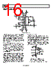
17 / 24 page  AD8253 Rev. 0 | Page 17 of 24 Table 5. Truth Table Logic Levels for Transparent Gain Mode WR A1 A0 Gain −VS Low Low 1 −VS Low High 10 −VS High Low 100 −VS High High 1000 Latched Gain Mode Some applications have multiple programmable devices such as multiplexers or other programmable gain instrumentation amplifiers on the same PCB. In such cases, devices can share a data bus. The gain of the AD8253 can be set using WR as a latch, allowing other devices to share A0 and A1. shows a schematic using this method, known as latched gain mode. The AD8253 is in this mode when Figure 53 WR is held at logic high or logic low, typically 5 V and 0 V, respectively. The voltages on A0 and A1 are read on the downward edge of the WR signal as it transitions from logic high to logic low. This latches in the logic levels on A0 and A1, resulting in a gain change. See the truth table listing in for more on these gain changes. Table 6 +15V –15V A0 A1 WR +IN –IN 10μF0.1µF 10μF0.1µF DGND DGND REF AD8253 A0 A1 WR +5V +5V +5V 0V 0V 0V G = PREVIOUS STATE G = 1000 + – NOTE: 1. ON THE DOWNWARD EDGE OF WR, AS IT TRANSITIONS FROM LOGIC HIGH TO LOGIC LOW, THE VOLTAGES ON A0 AND A1 ARE READ AND LATCHED IN, RESULTING IN A GAIN CHANGE. IN THIS EXAMPLE, THE GAIN SWITCHES TO G = 1000. Figure 53. Latched Gain Mode, G = 1000 Table 6. Truth Table Logic Levels for Latched Gain Mode WR A1 A0 Gain High to Low Low Low Change to 1 High to Low Low High Change to 10 High to Low High Low Change to 100 High to Low High High Change to 1000 Low to Low X1 X1 No change Low to High X1 X1 No change High to High X1 X1 No change 1 X = don’t care. On power-up, the AD8253 defaults to a gain of 1 when in latched gain mode. In contrast, if the AD8253 is configured in transparent gain mode, it starts at the gain indicated by the voltage levels on A0 and A1 on power-up. Timing for Latched Gain Mode In latched gain mode, logic levels at A0 and A1 must be held for a minimum setup time, tSU, before the downward edge of WR latches in the gain. Similarly, they must be held for a minimum hold time, tHD, after the downward edge of WR to ensure that the gain is latched in correctly. After tHD, A0 and A1 may change logic levels, but the gain does not change until the next downward edge of WR. The minimum duration that WR can be held high is t WR-HIGH, and t WR-LOW is the minimum duration that WR can be held low. Digital timing specifications are listed in The time required for a gain change is dominated by the settling time of the amplifier. A timing diagram is shown in . Table 2. Figure 54 When sharing a data bus with other devices, logic levels applied to those devices can potentially feed through to the output of the AD8253. Feedthrough can be minimized by decreasing the edge rate of the logic signals. Furthermore, careful layout of the PCB also reduces coupling between the digital and analog portions of the board. A0, A1 WR tSU tHD tWR-HIGH tWR-LOW Figure 54. Timing Diagram for Latched Gain Mode |
|
|
Link URL |
| Lei ha avuto il aiuto da alldatasheet? [ DONATE ] |
Di alldatasheet | Richest di pubblicita | contatti | Privacy Policy | Collegamento alla scheda tecnica | scambio Link | Ricerca produttore All Rights Reserved©Alldatasheet.com |
| Russian : Alldatasheetru.com | Korean : Alldatasheet.co.kr | Spanish : Alldatasheet.es | French : Alldatasheet.fr | Italian : Alldatasheetit.com Portuguese : Alldatasheetpt.com | Polish : Alldatasheet.pl | Vietnamese : Alldatasheet.vn Indian : Alldatasheet.in | Mexican : Alldatasheet.com.mx | British : Alldatasheet.co.uk | New Zealand : Alldatasheet.co.nz |
|
Family Site : ic2ic.com |
icmetro.com |
 Italian ▼
 English
 Chinese
 German
 Japanese
 Russian
 Korean
 Spanish
 French
 Italian
 Portuguese
 Polish
 Vietnamese
 Indian
 Mexican
 British
 New Zealand