|
Motore di ricerca datesheet componenti elettronici |
|
|
Motore di ricerca datesheet componenti elettronici |
|
MPC8377E Scheda tecnica(PDF) 47 Page - Freescale Semiconductor, Inc |
|
|
|||||||||||||||||||||||||||||
MPC8377E Scheda tecnica(HTML) 47 Page - Freescale Semiconductor, Inc |
|
|
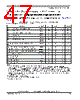
47 / 124 page  MPC8377E PowerQUICC™ II Pro Processor Hardware Specifications, Rev. 2 Freescale Semiconductor 47 Enhanced Secure Digital Host Controller (eSDHC) This means that Data + Clock delay must be greater than –2 ns. This is always fulfilled. 11.3 eSDHC AC Timing Specifications (High-Speed Mode) Table 42 provides the eSDHC AC timing specifications for high-speed mode as defined in Figure 30 and Figure 31. Table 42. eSDHC AC Timing Specifications for High-Speed Mode At recommended operating conditions OVDD = 3.3 V ± 165 mV. Parameter Symbol1 Min Max Unit Notes SD_CLK clock frequency—high speed mode fSHSCK 050 MHz — SD_CLK clock cycle tSFSCK 20 — ns — SD_CLK clock frequency—identification mode fSIDCK 0400 KHz — SD_CLK clock low time tSHSCKL 7— ns 2 SD_CLK clock high time tSHSCKH 7— ns 2 SD_CLK clock rise and fall times tSHSCKR/ tSHSCKF —3 ns 2 Input setup times: SD_CMD, SD_DATx, SD_CD to SD_CLK tSHSIVKH 5— ns 2 Input hold times: SD_CMD, SD_DATx, SD_CD to SD_CLK tSHSIXKH 0— ns 2 Output delay time: SD_CLK to SD_CMD, SD_DATx valid tSHSKHOV —4 ns 2 Output Hold time: SD_CLK to SD_CMD, SD_DATx invalid tSHSKHOX 0— ns 2 SD_CLK delay within device tINT_CLK_DLY 1.5 — ns 4 SD Card Input Setup tISU 6— ns 3 SD Card Input Hold tIH 2— ns 3 SD Card Output Valid tODLY —14 ns 3 SD Card Output Hold tOH 2.5 — ns 3 Note: 1 The symbols used for timing specifications herein follow the pattern of t (first three letters of functional block)(signal)(state) (reference)(state) for inputs and t(first three letters of functional block)(reference)(state)(signal)(state) for outputs. For example, tSFSIXKH symbolizes eSDHC full mode speed device timing (SFS) input (I) to go invalid (X) with respect to the clock reference (K) going to high (H). Also tSFSKHOV symbolizes eSDHC full speed timing (SFS) for the clock reference (K) to go high (H), with respect to the output (O) going valid (V) or data output valid time. Note that, in general, the clock reference symbol representation is based on five letters representing the clock of a particular functional. For rise and fall times, the latter convention is used with the appropriate letter: R (rise) or F (fall). 2 Measured at capacitive load of 40 pF. 3 For reference only, according to the SD card specifications. 4 Average, for reference only. |
|
Link URL |
| Lei ha avuto il aiuto da alldatasheet? [ DONATE ] |
Di alldatasheet | Richest di pubblicita | contatti | Privacy Policy | Collegamento alla scheda tecnica | scambio Link | Ricerca produttore All Rights Reserved©Alldatasheet.com |
| Russian : Alldatasheetru.com | Korean : Alldatasheet.co.kr | Spanish : Alldatasheet.es | French : Alldatasheet.fr | Italian : Alldatasheetit.com Portuguese : Alldatasheetpt.com | Polish : Alldatasheet.pl | Vietnamese : Alldatasheet.vn Indian : Alldatasheet.in | Mexican : Alldatasheet.com.mx | British : Alldatasheet.co.uk | New Zealand : Alldatasheet.co.nz |
|
Family Site : ic2ic.com |
icmetro.com |
 Italian ▼
 English
 Chinese
 German
 Japanese
 Russian
 Korean
 Spanish
 French
 Italian
 Portuguese
 Polish
 Vietnamese
 Indian
 Mexican
 British
 New Zealand