|
Motore di ricerca datesheet componenti elettronici |
|
|
Motore di ricerca datesheet componenti elettronici |
|
MPC8378E Scheda tecnica(PDF) 68 Page - Freescale Semiconductor, Inc |
|
|
|||||||||||||||||||||||||||||
MPC8378E Scheda tecnica(HTML) 68 Page - Freescale Semiconductor, Inc |
|
|
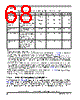
68 / 126 page  MPC8378E PowerQUICC™ II Pro Processor Hardware Specifications, Rev. 2 68 Freescale Semiconductor PCI Express 15.4.2 Transmitter Compliance Eye Diagrams The Tx eye diagram in Figure 46 is specified using the passive compliance/test measurement load (see Figure 48) in place of any real PCI Express interconnect + Rx component. There are two eye diagrams that must be met for the transmitter. Both diagrams must be aligned in time using the jitter median to locate the center of the eye diagram. The different eye diagrams differ in voltage depending on whether it is a Common mode return loss Measured over 50 MHz to 1.25 GHz. RLTX-CM 6— — dB 4 DC differential Tx impedance Tx DC differential mode low impedance ZTX-DIFF-DC 80 100 120 Ω — Transmitter DC impedance Required Tx D+ as well as D– DC impedance during all states ZTX-DC 40 — — Ω — Lane-to-Lane output skew Static skew between any two transmitter lanes within a single link LTX-SKEW — — 500 + 2UI ps — AC coupling capacitor All transmitters should be AC coupled. The AC coupling is required either within the media or within the transmitting component itself. CTX 75 — 200 nF — Crosslink random timeout This random timeout helps resolve conflicts in crosslink configuration by eventually resulting in only one downstream and one upstream port. Tcrosslink 0— 1 ms 7 Note: 1 No test load is necessarily associated with this value. 2 Specified at the measurement point into a timing and voltage compliance test load as shown in Figure 48 and measured over any 250 consecutive Tx UIs. (Also refer to the transmitter compliance eye diagram shown in Figure 46.) 3 A T TX-EYE = 0.70 UI provides for a total sum of deterministic and random jitter budget of TTX-JITTER-MAX = 0.30 UI for the transmitter collected over any 250 consecutive Tx UIs. The TTX-EYE-MEDIAN-to-MAX-JITTER median is less than half of the total Tx jitter budget collected over any 250 consecutive Tx UIs. It should be noted that the median is not the same as the mean. The jitter median describes the point in time where the number of jitter points on either side is approximately equal as opposed to the averaged time value. 4 The transmitter input impedance will result in a differential return loss greater than or equal to 12 dB and a common mode return loss greater than or equal to 6 dB over a frequency range of 50 MHz to 1.25 GHz. This input impedance requirement applies to all valid input levels. The reference impedance for return loss measurements is 50 Ω to ground for both the D+ and D– line (that is, as measured by a vector network analyzer with 50- Ω probes, see Figure 48). Note that the series capacitors, CTX, is optional for the return loss measurement. 5 Measured between 20%–80% at transmitter package pins into a test load as shown in Figure 48 for both V TX-D+ and VTX-D-. 6 See Section 4.3.1.8 of the PCI Express Base Specifications, Rev 1.0a. 7 See Section 4.2.6.3 of the PCI Express Base Specifications, Rev 1.0a. Table 56. Differential Transmitter (Tx) Output Specifications (continued) Parameter Conditions Symbol Min Typical Max Units Notes |
|
Link URL |
| Lei ha avuto il aiuto da alldatasheet? [ DONATE ] |
Di alldatasheet | Richest di pubblicita | contatti | Privacy Policy | Collegamento alla scheda tecnica | scambio Link | Ricerca produttore All Rights Reserved©Alldatasheet.com |
| Russian : Alldatasheetru.com | Korean : Alldatasheet.co.kr | Spanish : Alldatasheet.es | French : Alldatasheet.fr | Italian : Alldatasheetit.com Portuguese : Alldatasheetpt.com | Polish : Alldatasheet.pl | Vietnamese : Alldatasheet.vn Indian : Alldatasheet.in | Mexican : Alldatasheet.com.mx | British : Alldatasheet.co.uk | New Zealand : Alldatasheet.co.nz |
|
Family Site : ic2ic.com |
icmetro.com |
 Italian ▼
 English
 Chinese
 German
 Japanese
 Russian
 Korean
 Spanish
 French
 Italian
 Portuguese
 Polish
 Vietnamese
 Indian
 Mexican
 British
 New Zealand