|
Motore di ricerca datesheet componenti elettronici |
|
|
Motore di ricerca datesheet componenti elettronici |
|
MPC8378E Scheda tecnica(PDF) 119 Page - Freescale Semiconductor, Inc |
|
|
|||||||||||||||||||||||||||||
MPC8378E Scheda tecnica(HTML) 119 Page - Freescale Semiconductor, Inc |
|
|
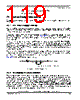
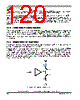
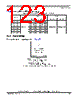
119 / 126 page  MPC8378E PowerQUICC™ II Pro Processor Hardware Specifications, Rev. 2 Freescale Semiconductor 119 System Design Information RθJC = junction to case thermal resistance (°C/W) PD = power dissipation (W) 24 System Design Information This section provides electrical and thermal design recommendations for successful application of the MPC8378E. 24.1 PLL Power Supply Filtering Each of the PLLs listed above is provided with power through independent power supply pins. The AVDD level should always be equivalent to VDD, and preferably these voltages will be derived directly from VDD through a low frequency filter scheme. There are a number of ways to reliably provide power to the PLLs, but the recommended solution is to provide five independent filter circuits as illustrated in Figure 68, one to each of the five AVDD pins. By providing independent filters to each PLL, the opportunity to cause noise injection from one PLL to the other is reduced. This circuit is intended to filter noise in the PLLs resonant frequency range from a 500 kHz to 10 MHz range. It should be built with surface mount capacitors with minimum Effective Series Inductance (ESL). Consistent with the recommendations of Dr. Howard Johnson in High Speed Digital Design: A Handbook of Black Magic (Prentice Hall, 1993), multiple small capacitors of equal value are recommended over a single large value capacitor. Each circuit should be placed as close as possible to the specific AVDD pin being supplied to minimize noise coupled from nearby circuits. It should be possible to route directly from the capacitors to the AVDD pin, which is on the periphery of package, without the inductance of vias. Figure 68 shows the PLL power supply filter circuit. Figure 68. PLL Power Supply Filter Circuit 24.2 Decoupling Recommendations Due to large address and data buses, and high operating frequencies, the device can generate transient power surges and high frequency noise in its power supply, especially while driving large capacitive loads. This noise must be prevented from reaching other components in the device system, and the device itself requires a clean, tightly regulated source of power. Therefore, it is recommended that the system designer place at least one decoupling capacitor at each VDD, OVDD, GVDD, and LVDD pins of the device. These decoupling capacitors should receive their power from separate VDD, OVDD, GVDD, LVDD, and GND power planes in the PCB, utilizing short traces to minimize inductance. Capacitors may be placed directly under the device using a standard escape pattern. Others may surround the part. VDD AVDD (or L2AVDD) 2.2 µF 2.2 µF GND Low ESL Surface Mount Capacitors 10 Ω |
|
Link URL |
| Lei ha avuto il aiuto da alldatasheet? [ DONATE ] |
Di alldatasheet | Richest di pubblicita | contatti | Privacy Policy | Collegamento alla scheda tecnica | scambio Link | Ricerca produttore All Rights Reserved©Alldatasheet.com |
| Russian : Alldatasheetru.com | Korean : Alldatasheet.co.kr | Spanish : Alldatasheet.es | French : Alldatasheet.fr | Italian : Alldatasheetit.com Portuguese : Alldatasheetpt.com | Polish : Alldatasheet.pl | Vietnamese : Alldatasheet.vn Indian : Alldatasheet.in | Mexican : Alldatasheet.com.mx | British : Alldatasheet.co.uk | New Zealand : Alldatasheet.co.nz |
|
Family Site : ic2ic.com |
icmetro.com |
 Italian ▼
 English
 Chinese
 German
 Japanese
 Russian
 Korean
 Spanish
 French
 Italian
 Portuguese
 Polish
 Vietnamese
 Indian
 Mexican
 British
 New Zealand