|
Motore di ricerca datesheet componenti elettronici |
|
|
Motore di ricerca datesheet componenti elettronici |
|
CXP83508 Scheda tecnica(PDF) 7 Page - Sony Corporation |
|
|
|||||||||||||||||||||||||||||
CXP83508 Scheda tecnica(HTML) 7 Page - Sony Corporation |
|
|
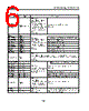
7 / 30 page  – 7 – CXP83508/83512/83516, CXP83509/83513/83517 Symbol I/O Functions Output/Output PF0/SEG24 to PF7/SEG31 (Port F) 8-bit output port. (8 pins) Output/Output PD0/SEG16 to PD7/SEG23 (Port D) 8-bit output port. (8 pins) Output SEG0 to SEG15 LCD segment signal output. (16 pins) Input Crystal connectors for system clock oscillation. When the clock is supplied externally, input to EXTAL; opposite phase clock should be input to XTAL. EXTAL Output COM0 to COM3 LCD common signal output. (4 pins) VLC1 to VLC3 LCD bias power supply. (3 pins) Output VL Control pin to cut off the current flowing to external LCD bias resistor during standby. XTAL Input Low-level active system reset. NC. Do not make any connections to NC. Positive power supply. GND. RST NC VDD VSS LCD segment signal outputs. (16 pins) |
|
Link URL |
| Lei ha avuto il aiuto da alldatasheet? [ DONATE ] |
Di alldatasheet | Richest di pubblicita | contatti | Privacy Policy | Collegamento alla scheda tecnica | scambio Link | Ricerca produttore All Rights Reserved©Alldatasheet.com |
| Russian : Alldatasheetru.com | Korean : Alldatasheet.co.kr | Spanish : Alldatasheet.es | French : Alldatasheet.fr | Italian : Alldatasheetit.com Portuguese : Alldatasheetpt.com | Polish : Alldatasheet.pl | Vietnamese : Alldatasheet.vn Indian : Alldatasheet.in | Mexican : Alldatasheet.com.mx | British : Alldatasheet.co.uk | New Zealand : Alldatasheet.co.nz |
|
Family Site : ic2ic.com |
icmetro.com |
 Italian ▼
 English
 Chinese
 German
 Japanese
 Russian
 Korean
 Spanish
 French
 Italian
 Portuguese
 Polish
 Vietnamese
 Indian
 Mexican
 British
 New Zealand