|
Motore di ricerca datesheet componenti elettronici |
|
|
Motore di ricerca datesheet componenti elettronici |
|
IDT7M1001S40C Scheda tecnica(PDF) 5 Page - Integrated Device Technology |
|
|
|||||||||||||||||||||||||||||
IDT7M1001S40C Scheda tecnica(HTML) 5 Page - Integrated Device Technology |
|
|
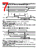
5 / 11 page  IDT7M1001/1003 128K/64K x 8 CMOS DUAL-PORT STATIC RAM MODULE MILITARY AND COMMERCIAL TEMPERATURE RANGES 7.5 5 AC ELECTRICAL CHARACTERISTICS (VCC = 5.0V ± 10%, TA = -55°C to +125°C and 0°C to +70°C) –35 –40 –50 Symbol Parameter Min. Max. Min. Max. Min. Max. Unit Read Cycle tRC Read Cycle Time 35 — 40 — 50 — ns tAA Address Access Time — 35 — 40 — 50 ns tACS (2) Chip Select Access Time — 35 — 40 — 50 ns tOE Output Enable Access Time — 20 — 25 — 30 ns tOH Output Hold From Address Change 3 — 3 — 3 — ns tCLZ (1) Chip Select to Output in Low-Z 3 — 3 — 3 — ns tCHZ (1) Chip Deselect to Output in High-Z — 20 — 20 — 25 ns tOLZ (1) Output Enable to Output in Low-Z 3 — 3 — 3 — ns tOHZ (1) Output Disable to Output in High-Z — 20 — 20 — 25 ns tPU (1) Chip Select to Power-Up Time 0 — 0 — 0 — ns tPD (1) Chip Disable to Power-Down Time — 50 — 50 — 50 ns tSOP SEM Flag Update Pulse (OE or SEM) 15 — 15 — 15 — ns Write Cycle tWC Write Cycle Time 35 — 40 — 50 — ns tCW (2) Chip Select to End-of-Write 30 — 35 — 40 — ns tAW Address Valid to End-of-Write 30 — 35 — 40 — ns tAS1 (3) Address Set-up to Write Pulse Time 5 — 5 — 5 — ns tAS2 Address Set-up to CS Time 0 — 0 — 0 — ns tWP Write Pulse Width 30 — 35 — 40 — ns tWR (4) Write Recovery Time 0 — 0 — 0 — ns tDW Data Valid to End-of-Write 25 — 30 — 35 — ns tDH (4) Data Hold Time 0 — 0 — 0 — ns tOHZ (1) Output Disable to Output in High-Z — 20 — 20 — 25 ns tWHZ (1) Write Enable to Output in High-Z — 20 — 20 — 25 ns tOW (1, 4) Output Active from End-of-Write 0 — 0 — 0 — ns tSWRD SEM Flag Write to Read Time 15 — 15 — 15 — ns tSPS SEM Flag Contention Window 15 — 15 — 15 — ns Port-to-Port Delay Timing tWDD (5) Write Pulse to Data Delay — 60 — 65 — 70 ns tDDD (5) Write Data Valid to Read Data Valid — 45 — 50 — 55 ns NOTES: 1. This parameter is guaranteed by design but not tested. 2. To access RAM CS ≤ VIL and SEM ≥ VIH. To access semaphore, CS ≥ VIH and SEM ≤ VIL. 3. tAS1= 0 if R/ W is asserted LOW simultaneously with or after the CS LOW transition. 4. For CS controlled write cycles, tWR= 5ns, tDH= 5ns, tOW= 5ns. 5. Port-to-Port delay through the RAM cells from the writing port to the reading port. 2804 tbl 09 |
|
|
Link URL |
| Lei ha avuto il aiuto da alldatasheet? [ DONATE ] |
Di alldatasheet | Richest di pubblicita | contatti | Privacy Policy | Collegamento alla scheda tecnica | scambio Link | Ricerca produttore All Rights Reserved©Alldatasheet.com |
| Russian : Alldatasheetru.com | Korean : Alldatasheet.co.kr | Spanish : Alldatasheet.es | French : Alldatasheet.fr | Italian : Alldatasheetit.com Portuguese : Alldatasheetpt.com | Polish : Alldatasheet.pl | Vietnamese : Alldatasheet.vn Indian : Alldatasheet.in | Mexican : Alldatasheet.com.mx | British : Alldatasheet.co.uk | New Zealand : Alldatasheet.co.nz |
|
Family Site : ic2ic.com |
icmetro.com |
 Italian ▼
 English
 Chinese
 German
 Japanese
 Russian
 Korean
 Spanish
 French
 Italian
 Portuguese
 Polish
 Vietnamese
 Indian
 Mexican
 British
 New Zealand