|
Motore di ricerca datesheet componenti elettronici |
|
|
Motore di ricerca datesheet componenti elettronici |
|
AS4DDR232M72APBG Scheda tecnica(PDF) 3 Page - Micross Components |
|
|
|||||||||||||||||||||||||||||
AS4DDR232M72APBG Scheda tecnica(HTML) 3 Page - Micross Components |
|
|
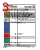
3 / 28 page  iPEM 2.4 Gb SDRAM-DDR2 AS4DDR232M72APBG AS4DDR232M72APBG Rev. 1.1 12/12 3 Micross Components reserves the right to change products or specifications without notice. BGA Locations Symbol Type Description L6 ODT CNTL Input On-Die-Termination: Registered High enables on data bus termination F4, F16, G5, G15, K12 CKx, CKx\ CNTL Input Differential input clocks, one set for each x16bits L13, L2, K1, M8, N6 G4, G16, K13, M6, K2 CKEx CNTL Input Clock enable which activates all on silicon clocking circuitry G1, G13, K16, K4, M12 CSx\ CNTL Input Chip Selects, one for each 16 bits of the data bus width F12, G2, K15, L5, M11 RASx\ CNTL Input Command input which along with CAS\, WE\ and CS\ define operations F1, G12, M9, L16, L4, CASx\ CNTL Input Command input which along with RAS\, WE\ and CS\ define operations F2, F13, L15, M4, M10 Wex\ CNTL Input Command input which along with RAS\, CAS\ and CS\ define operations E4, F15, M13, M7, M2 UDMx CNTL Input One Data Mask cntl. for each upper 8 bits of a x16 word E2, E13, M15, M5, N11 LDMx CNTL Input One Data Mask cntl. For each lower 8 bits of a x16 word E5, E7, E11, N12, N5 UDQSx CNTL Input Data Strobe input for upper byte of each x16 word F6, F8, F10, K6, L11 UDQSx\ CNTL Input Differential input of UDQSx, only used when Differential DQS mode is enabled E6, E10, F5, K5, L12 LDQSx CNTL Input Data Strobe input for lower byte of each x16 word F7, F11, G6, L7, L10 LDQSx\ CNTL Input Differential input of LDQSx, only used when Differential DQS mode is enabled A7, A8, A9, A10, B7, Ax Input Array Address inputs providing ROW addresses for Active commands, and B8, B9, B10, C7, C8, the column address and auto precharge bit (A10) for READ/WRITE commands C9, C10, D7 D8, D9, D10 DNU Future Input E8, E9 BA0, BA1 Input Bank Address inputs A2, A3, A4, A13, A14, DQx Input/Output Data bidirectional input/Output pins A15, B1, B2, B3, B4, B13, B14, B15, B16, C1, C2, C3, C4, C13, C14, C15, C16, D1, D2, D3, D4, D13, D14, D15, D16, E1, E16, M1, M16, N1, N2, N3, N4, N7, N8, N9, N10, N13, N14, N15, N16, PP1, P2, P3, P4, P7, P8, P9, P10, P13, P14, P15, P16, R1, R2, R3, R4, R7, R8, R9, R10, R13, R14, R15, R16, T2, T3, T4, T7, T8, T9, T10, T13, T14, T15 E12 Vref Supply SSTL_18 Voltage Reference B11, B12, C5, C6,E3, VCC Supply Core Power Supply F3, G3, H3, H12, H16, J3, J12, J16, K3, L3, M3, P11, P12, R5, R6, T16 A11, A12, D5, D6, H4, VCCQ Supply I/O Power H15, J4, J15, T5, T6 A5, A6, A16, B5, B6, VSS Supply Core Ground return C11, C12, D11, D12, E14, F14, G14, H1, H2, H14, J1, J2, J5, J13, J14, K14, L14, M14, P5, P6, R11, R12, T1, T11, T12, H5, H13 G7, G8, G9, G10, H7, VSSQ Supply I/O Ground return H8, H9, H10, J7, J8, J9, J10, K7, K8, K9, K10 E15, F9, G11, H6, H11, NC No connection J6, J11, K11, L1, L8, L9, A1 UNPOPULATED Unpopulated ball matrix location (location registration aid) |
|
Link URL |
| Lei ha avuto il aiuto da alldatasheet? [ DONATE ] |
Di alldatasheet | Richest di pubblicita | contatti | Privacy Policy | Collegamento alla scheda tecnica | scambio Link | Ricerca produttore All Rights Reserved©Alldatasheet.com |
| Russian : Alldatasheetru.com | Korean : Alldatasheet.co.kr | Spanish : Alldatasheet.es | French : Alldatasheet.fr | Italian : Alldatasheetit.com Portuguese : Alldatasheetpt.com | Polish : Alldatasheet.pl | Vietnamese : Alldatasheet.vn Indian : Alldatasheet.in | Mexican : Alldatasheet.com.mx | British : Alldatasheet.co.uk | New Zealand : Alldatasheet.co.nz |
|
Family Site : ic2ic.com |
icmetro.com |
 Italian ▼
 English
 Chinese
 German
 Japanese
 Russian
 Korean
 Spanish
 French
 Italian
 Portuguese
 Polish
 Vietnamese
 Indian
 Mexican
 British
 New Zealand