|
Motore di ricerca datesheet componenti elettronici |
|
|
Motore di ricerca datesheet componenti elettronici |
|
ADP199ACBZ-R7 Scheda tecnica(PDF) 1 Page - Analog Devices |
|
|
|||||||||||||||||||||||||||||
ADP199ACBZ-R7 Scheda tecnica(HTML) 1 Page - Analog Devices |
|
|
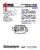
1 / 16 page  3.6 V, 500 mA Logic Controlled High-Side Load Switch Data Sheet ADP199 Rev. 0 Information furnished by Analog Devices is believed to be accurate and reliable. However, no responsibilityis assumedbyAnalogDevicesforitsuse,norforanyinfringements of patents or other rightsofthirdpartiesthatmayresultfromitsuse.Specificationssubjecttochangewithoutnotice.No license is granted by implication or otherwise under any patent or patent rights of Analog Devices. Trademarksandregisteredtrademarksarethepropertyoftheirrespectiveowners. One Technology Way, P.O. Box 9106, Norwood, MA 02062-9106, U.S.A. Tel: 781.329.4700 www.analog.com Fax: 781.461.3113 ©2011 Analog Devices, Inc. All rights reserved. FEATURES Constant low RDSON of 40 mΩ over input voltage range Low input voltage range: 0.9 V to 3.6 V 500 mA continuous operating current at 85°C 1.2 V logic compatible enable input Low 6 μA quiescent current, independent of load current Ultralow shutdown current: <100 nA Ultrasmall 0.8 mm × 0.8 mm × 0.5 mm, 4-ball, 0.4 mm pitch WLCSP APPLICATIONS Low operating voltage processors Mobile phones Digital cameras and audio devices Portable and battery-powered equipment Optical XMT/RCVR modules GENERAL DESCRIPTION The ADP199 is a high-side load switch designed for opera- tion between 0.9 V to 3.6 V. A load switch provides power domain isolation, thereby helping to keep subsystems isolated and powered independently, and enabling reduced power consumption. The ADP199 contains a low on-resistance, N-channel MOSFET to minimize power loss, and supports over 500 mA of continuous load current. The low 6 μA quiescent current and ultralow shutdown current make the ADP199 ideal for battery-operated portable equipment. The built-in level shifter for enable logic makes the ADP199 compatible with many processors and GPIO controllers. In addition to high performance, the ADP199 occupies mini- mal printed circuit board (PCB) space with an area of less than 0.64 mm2 and a height of 0.50 mm. The ADP199 is available in an ultra-small, 0.8 mm × 0.8 mm × 0.5 mm, 4-ball, 0.4 mm pitch WLCSP. TYPICAL APPLICATIONS CIRCUIT GND EN LOAD VIN VOUT ADP199 CHARGE PUMP AND SLEW RATE CONTROL OFF ON + – 4Ω Figure 1. |
Codice articolo simile - ADP199ACBZ-R7 |
|
Descrizione simile - ADP199ACBZ-R7 |
|
|
|
Link URL |
| Lei ha avuto il aiuto da alldatasheet? [ DONATE ] |
Di alldatasheet | Richest di pubblicita | contatti | Privacy Policy | Collegamento alla scheda tecnica | scambio Link | Ricerca produttore All Rights Reserved©Alldatasheet.com |
| Russian : Alldatasheetru.com | Korean : Alldatasheet.co.kr | Spanish : Alldatasheet.es | French : Alldatasheet.fr | Italian : Alldatasheetit.com Portuguese : Alldatasheetpt.com | Polish : Alldatasheet.pl | Vietnamese : Alldatasheet.vn Indian : Alldatasheet.in | Mexican : Alldatasheet.com.mx | British : Alldatasheet.co.uk | New Zealand : Alldatasheet.co.nz |
|
Family Site : ic2ic.com |
icmetro.com |
 Italian ▼
 English
 Chinese
 German
 Japanese
 Russian
 Korean
 Spanish
 French
 Italian
 Portuguese
 Polish
 Vietnamese
 Indian
 Mexican
 British
 New Zealand