|
Motore di ricerca datesheet componenti elettronici |
|
|
Motore di ricerca datesheet componenti elettronici |
|
ADP199ACBZ-R7 Scheda tecnica(PDF) 12 Page - Analog Devices |
|
|
|||||||||||||||||||||||||||||
ADP199ACBZ-R7 Scheda tecnica(HTML) 12 Page - Analog Devices |
|
|
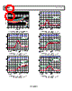
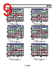
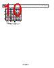
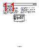
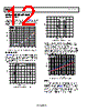
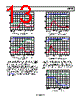
12 / 16 page  ADP199 Data Sheet Rev. 0 | Page 12 of 16 APPLICATIONS INFORMATION GROUND CURRENT The major source for ground current in the ADP199 is the internal charge pump for the FET drive circuitry. Figure 30 shows the typical ground current when VEN = VIN, and varies from 1.1 V to 3.6 V. 0 5 10 15 20 25 30 35 40 45 50 0.8 1.2 1.6 2.0 2.4 2.8 3.2 3.6 VIN (V) 5mA 10mA 50mA 100mA 200mA 500mA Figure 30. Ground Current vs. Input Voltage, Different Load Current ENABLE FEATURE The ADP199 uses the EN input to enable and disable the VOUT output. As shown in Figure 31, when a rising voltage (VEN) on the EN pin crosses the active threshold, VOUT turns on. When a falling voltage (VEN) on the EN pin crosses the inactive threshold, VOUT turns off. 0 0.5 1.0 1.5 2.0 2.5 3.0 3.5 1.21.3 1.41.51.61.7 1.81.92.02.1 ENABLE VOLTAGE (V) VOUT AT 3.3V Figure 31. Typical EN Operation, VIN = 3.3 V ENABLE VOLTAGE (V) 0 0.2 0.4 0.6 0.8 1.0 1.2 1.4 0.30 0.35 0.40 0.45 0.50 0.55 0.60 0.65 0.70 VOUT AT 1.2V Figure 32. Typical EN Operation, VIN = 1.2 V As shown in Figure 31, the EN pin has hysteresis built into it. This prevents on/off oscillations that can occur due to noise on the EN pin as it passes through the threshold points. The EN pin active/inactive thresholds derive from the VIN voltage; therefore, these thresholds vary with the changing input voltage. Figure 33 shows the typical EN active/inactive thresholds when the input voltage varies from 1.1 V to 3.6 V. 0 0.5 1.0 1.5 2.0 2.5 1.0 1.5 2.0 2.5 3.0 3.5 INPUT VOLTAGE (V) EN RISE EN FALL Figure 33. Typical EN Thresholds vs. Input Voltage (VIN) TIMING Turn-on delay is defined as the interval between the time that VEN exceeds the rising threshold voltage and when VOUT rises to ~10% of its final value. The ADP199 includes circuitry that has a typical 1 ms turn-on delay, and a controlled rise time to limit the VIN inrush current. As shown in Figure 34 and Figure 35, the turn- on delay is nearly independent of the input voltage. |
|
|
Link URL |
| Lei ha avuto il aiuto da alldatasheet? [ DONATE ] |
Di alldatasheet | Richest di pubblicita | contatti | Privacy Policy | Collegamento alla scheda tecnica | scambio Link | Ricerca produttore All Rights Reserved©Alldatasheet.com |
| Russian : Alldatasheetru.com | Korean : Alldatasheet.co.kr | Spanish : Alldatasheet.es | French : Alldatasheet.fr | Italian : Alldatasheetit.com Portuguese : Alldatasheetpt.com | Polish : Alldatasheet.pl | Vietnamese : Alldatasheet.vn Indian : Alldatasheet.in | Mexican : Alldatasheet.com.mx | British : Alldatasheet.co.uk | New Zealand : Alldatasheet.co.nz |
|
Family Site : ic2ic.com |
icmetro.com |
 Italian ▼
 English
 Chinese
 German
 Japanese
 Russian
 Korean
 Spanish
 French
 Italian
 Portuguese
 Polish
 Vietnamese
 Indian
 Mexican
 British
 New Zealand