|
Motore di ricerca datesheet componenti elettronici |
|
|
Motore di ricerca datesheet componenti elettronici |
|
HT48R30A Scheda tecnica(PDF) 4 Page - Holtek Semiconductor Inc |
|
|
|||||||||||||||||||||||||||||
HT48R30A Scheda tecnica(HTML) 4 Page - Holtek Semiconductor Inc |
|
|
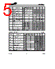
4 / 43 page  Pin Name I/O ROM Code Option Description RES I ¾ Schmitt trigger reset input. Active low VDD ¾¾ Positive power supply OSC1/PG1 OSC2/PG2 I O Pull-high* Crystal or RC or Int. RC+I/O or Int. RC+RTC OSC1, OSC2 are connected to an RC network or Crystal (deter- mined by ROM code option) for the internal system clock. In the case of RC operation, OSC2 is the output terminal for 1/4 sys- tem clock. These two pins can also be optioned as an RTC oscil- lator (32768Hz) or I/O lines. In these two cases, the system clock comes from an internal RC oscillator whose frequency has 4 options (3.2MHz, 1.6MHz, 800kHz, 400kHz). If the I/O option is selected, the pull-high options can also be enabled or dis- abled. Otherwise the PG1 and PG2 are used as internal regis- ters (pull-high resistors are always disabled). Note: ²*² The pull-high resistors of each I/O port (PA, PB, PC, PG) are controlled by 1-bit ROM code option. CMOS or Schmitt trigger option of port A is controlled by 1-bit ROM code option. Absolute Maximum Ratings Supply Voltage ...............VSS-0.3V to VSS+5.5V Storage Temperature ................-50°Cto125°C Input Voltage.................VSS-0.3V to VDD+0.3V Operating Temperature ..............-40°Cto85°C Note: These are stress ratings only. Stresses exceeding the range specified under "Absolute Maxi- mum Ratings" may cause substantial damage to the device. Functional operation of this device at other conditions beyond those listed in the specification is not implied and prolonged expo- sure to extreme conditions may affect device reliability. D.C. Characteristics Ta=25°C Symbol Parameter Test Conditions Min. Typ. Max. Unit VDD Conditions VDD1 Operating Voltage ¾ fSYS=4MHz 3.3 ¾ 5.5 V VDD2 Operating Voltage ¾ fSYS=8MHz 4.5 ¾ 5.5 V IDD1 Operating Current (Crystal OSC) 3.3V No load, fSYS=4MHz ¾ 12 mA 5V ¾ 35 mA IDD2 Operating Current (RC OSC) 3.3V No load, fSYS=4MHz ¾ 12 mA 5V ¾ 35 mA IDD3 Operating Current (Crystal OSC) 5V No load, fSYS=8MHz ¾ 48 mA ISTB1 Standby Current (WDT Enabled RTC Off) 3.3V No load, system HALT ¾¾ 5 mA 5V ¾¾ 10 mA HT48R30A-1 Rev. 1.10 4 July 2, 2001 |
|
Link URL |
| Lei ha avuto il aiuto da alldatasheet? [ DONATE ] |
Di alldatasheet | Richest di pubblicita | contatti | Privacy Policy | Collegamento alla scheda tecnica | scambio Link | Ricerca produttore All Rights Reserved©Alldatasheet.com |
| Russian : Alldatasheetru.com | Korean : Alldatasheet.co.kr | Spanish : Alldatasheet.es | French : Alldatasheet.fr | Italian : Alldatasheetit.com Portuguese : Alldatasheetpt.com | Polish : Alldatasheet.pl | Vietnamese : Alldatasheet.vn Indian : Alldatasheet.in | Mexican : Alldatasheet.com.mx | British : Alldatasheet.co.uk | New Zealand : Alldatasheet.co.nz |
|
Family Site : ic2ic.com |
icmetro.com |
 Italian ▼
 English
 Chinese
 German
 Japanese
 Russian
 Korean
 Spanish
 French
 Italian
 Portuguese
 Polish
 Vietnamese
 Indian
 Mexican
 British
 New Zealand