|
Motore di ricerca datesheet componenti elettronici |
|
|
Motore di ricerca datesheet componenti elettronici |
|
MCP3202 Scheda tecnica(PDF) 15 Page - Microchip Technology |
|
|
|||||||||||||||||||||||||||||
MCP3202 Scheda tecnica(HTML) 15 Page - Microchip Technology |
|
|
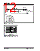
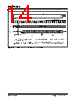
15 / 28 page  © 2006 Microchip Technology Inc. DS21034D-page 15 MCP3202 6.0 APPLICATIONS INFORMATION 6.1 Using the MCP3202 with Microcontroller (MCU) SPI Ports With most microcontroller SPI ports, it is required to send groups of eight bits. It is also required that the microcontroller SPI port be configured to clock out data on the falling edge of clock and latch data in on the ris- ing edge. Depending on how communication routines are used, it is very possible that the number of clocks required for communication will not be a multiple of eight. Therefore, it may be necessary for the MCU to send more clocks than are actually required. This is usually done by sending ‘leading zeros’ before the start bit, which are ignored by the device. As an example, Figure 6-1 and Figure 6-2 show how the MCP3202 can be interfaced to a MCU with a hardware SPI port. Figure 6-1 depicts the operation shown in SPI Mode 0,0, which requires that the SCLK from the MCU idles in the ‘low’ state, while Figure 6-2 shows the similar case of SPI Mode 1,1 where the clock idles in the ‘high’ state. As shown in Figure 6-1, the first byte transmitted to the A/D Converter contains seven leading zeros before the start bit. Arranging the leading zeros this way produces the output 12 bits to fall in positions easily manipulated by the MCU. The MSB is clocked out of the A/D Con- verter on the falling edge of clock number 12. After the second eight clocks have been sent to the device, the MCU receive buffer will contain three unknown bits (the output is at high impedance until the null bit is clocked out), the null bit and the highest order four bits of the conversion. After the third byte has been sent to the device, the receive register will contain the lowest order eight bits of the conversion results. Easier manipulation of the converted data can be obtained by using this method. FIGURE 6-1: SPI Communication using 8-bit segments (Mode 0,0: SCLK idles low). FIGURE 6-2: SPI Communication using 8-bit segments (Mode 1,1: SCLK idles high). 1 2 3 4 5 6 7 8 9 10 11 1213 1415 16 CS SCLK D IN X = Don’t Care Bits 17 18 19 20 21 22 23 24 D OUT NULL BIT B11 B10 B9 B8 B7 B6 B5 B4 B3 B2 B1 B0 HI-Z MCU latches data from A/D Converter Data is clocked out of A/D Converter on falling edges on rising edges of SCLK Don’t Care Start XX X X X XX X X X X X XX X X XX B7 B6 B5 B4 B3 B2 B1 B0 B11 B10 B9 B8 0 X X X X X X X X X X X 1 Start Bit (Null) MCU Transmitted Data (Aligned with falling edge of clock) MCU Received Data (Aligned with rising edge of clock) MSBF SGL/ DIFF XX SGL/ DIFF ODD/ SIGN Data stored into MCU receive register after transmission of first 8 bits Data stored into MCU receive register after transmission of second 8 bits Data stored into MCU receive register after transmission of last 8 bits 12 3 4 5 6 7 8 9 10 11 12 13 14 15 16 CS SCLK D IN X = Don’t Care Bits 17 18 19 20 21 22 23 24 D OUT Don’t Care NULL BIT B11 B10 B9 B8 B6 B5 B4 B3 B2 B1 B0 HI-Z 00 0 0 0 0 XX X X X X X XX X X XX B7 B6 B5 B4 B3 B2 B1 B0 B11 B10 B9 B8 0 X XXXXX XX XXX MCU latches data from A/D Converter on rising edges of SCLK Data is clocked out of A/D Converter on falling edges Start Bit (Null) Start MCU Transmitted Data (Aligned with falling edge of clock) MCU Received Data (Aligned with rising edge of clock) B7 1 0 SGL/ DIFF ODD/ SIGN MSBF Data stored into MCU receive register after transmission of first 8 bits Data stored into MCU receive register after transmission of second 8 bits Data stored into MCU receive register after transmission of last 8 bits |
|
Link URL |
| Lei ha avuto il aiuto da alldatasheet? [ DONATE ] |
Di alldatasheet | Richest di pubblicita | contatti | Privacy Policy | Collegamento alla scheda tecnica | scambio Link | Ricerca produttore All Rights Reserved©Alldatasheet.com |
| Russian : Alldatasheetru.com | Korean : Alldatasheet.co.kr | Spanish : Alldatasheet.es | French : Alldatasheet.fr | Italian : Alldatasheetit.com Portuguese : Alldatasheetpt.com | Polish : Alldatasheet.pl | Vietnamese : Alldatasheet.vn Indian : Alldatasheet.in | Mexican : Alldatasheet.com.mx | British : Alldatasheet.co.uk | New Zealand : Alldatasheet.co.nz |
|
Family Site : ic2ic.com |
icmetro.com |
 Italian ▼
 English
 Chinese
 German
 Japanese
 Russian
 Korean
 Spanish
 French
 Italian
 Portuguese
 Polish
 Vietnamese
 Indian
 Mexican
 British
 New Zealand