|
Motore di ricerca datesheet componenti elettronici |
|
|
Motore di ricerca datesheet componenti elettronici |
|
AD8009JRT-R2 Scheda tecnica(PDF) 13 Page - Analog Devices |
|
|
|||||||||||||||||||||||||||||
AD8009JRT-R2 Scheda tecnica(HTML) 13 Page - Analog Devices |
|
|
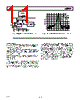
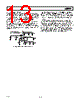
13 / 16 page  –13– REV. F AD8009 Driving a Capacitive Load A capacitive load, like that presented by some A/D converters, can sometimes be a challenge for an op amp to drive depending on the architecture of the op amp. Most of the problem is caused by the pole created by the output impedance of the op amp and the capacitor that is driven. This creates extra phase shift that can eventually cause the op amp to become unstable. One way to prevent instability and improve settling time when driving a capacitor is to insert a resistor in series between the op amp output and the capacitor. The feedback resistor is still connected directly to the output of the op amp, while the series resistor provides some isolation of the capacitive load from the op amp output. 10 F + 0.1 F 0.001 F 10 F + 0.1 F 0.001 F AD8009 49.9 +5V –5V 3 2 4 RT RS CL 50pF 2VSTEP 7 6 RF RG G = +2: RF = 301 = RG G = +10: RF = 200 , RG = 22.1 Figure 5. Capacitive Load Drive Circuit Figure 5 shows such a circuit with an AD8009 driving a 50 pF load. With RS = 0, the AD8009 circuit will be unstable. For a gain of +2 and +10, it was found experimentally that setting RS to 42.2 Ω will minimize the 0.1% settling time with a 2 V step at the output. The 0.1% settling time was measured to be 40 ns with this circuit. For smaller capacitive loads, a smaller RS will yield optimal settling time, while a larger RS will be required for larger capacitive loads. Of course, a larger capacitance will always require more time for settling to a given accuracy than a smaller one, and this will be lengthened by the increase in RS required. At best, a given RC combination will require about seven time constants by itself to settle to 0.1%, so a limit will be reached where too large a capacitance cannot be driven by a given op amp and still meet the system’s required settling time specification. |
|
|
Link URL |
| Lei ha avuto il aiuto da alldatasheet? [ DONATE ] |
Di alldatasheet | Richest di pubblicita | contatti | Privacy Policy | Collegamento alla scheda tecnica | scambio Link | Ricerca produttore All Rights Reserved©Alldatasheet.com |
| Russian : Alldatasheetru.com | Korean : Alldatasheet.co.kr | Spanish : Alldatasheet.es | French : Alldatasheet.fr | Italian : Alldatasheetit.com Portuguese : Alldatasheetpt.com | Polish : Alldatasheet.pl | Vietnamese : Alldatasheet.vn Indian : Alldatasheet.in | Mexican : Alldatasheet.com.mx | British : Alldatasheet.co.uk | New Zealand : Alldatasheet.co.nz |
|
Family Site : ic2ic.com |
icmetro.com |
 Italian ▼
 English
 Chinese
 German
 Japanese
 Russian
 Korean
 Spanish
 French
 Italian
 Portuguese
 Polish
 Vietnamese
 Indian
 Mexican
 British
 New Zealand