|
Motore di ricerca datesheet componenti elettronici |
|
|
Motore di ricerca datesheet componenti elettronici |
|
MIC2174 Scheda tecnica(PDF) 10 Page - Micrel Semiconductor |
|
|
|||||||||||||||||||||||||||||
MIC2174 Scheda tecnica(HTML) 10 Page - Micrel Semiconductor |
|
|
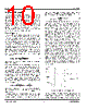
10 / 24 page  Micrel, Inc. MIC2174 September 2009 10 M9999-090409-B Functional Description The MIC2174 is an adaptive on-time synchronous buck controller built for low cost and high performance. It is designed for wide input voltage range from 3V to 40V and for high output power buck converters. An estimated-ON-time method is applied in MIC2174 to obtain a constant switching frequency and to simplify the control compensation. The over-current protection is implemented without the use of an external sense resistor. It includes an internal soft-start function which reduces the power supply input surge current at start-up by controlling the output voltage rise time. Theory of Operation The MIC2174 is an adaptive on-time buck controller. Figure 1 illustrates the block diagram for the control loop. The output voltage variation will be sensed by the MIC2174 feedback pin FB via the voltage divider R1 and R2, and compared to a 0.8V reference voltage VREF at the error comparator through a low gain transconductance (gm) amplifier, which improves the MIC2174 converter output voltage regulation. If the FB voltage decreases and the output of the gm amplifier is below 0.8V, the error comparator will trigger the control logic and generate an ON-time period, in which DH pin is logic high and DL pin is logic low. The ON-time period length is predetermined by the “FIXED TON ESTIMATION” circuitry: 300kHz V V T HSD OUT ed) ON(estimat × = (1) where VOUT is the output voltage, VHSD is the power stage input voltage. After ON-time period, the MIC2174 goes into the OFF- time period. In which DH pin is logic low and DL pin is logic high. The OFF-time period length depends upon the FB voltage in most cases. When the FB voltage decreases and the output of the gm amplifier is below 0.8V, the ON-time period is trigger and the OFF-time period ends. If the OFF-time period decided by the FB voltage is less than the minimum OFF time TOFF(min), which is about 363ns typical, the MIC2174 control logic will apply the TOFF(min) instead. TOFF(min) is required by the BST charging. The maximum duty cycle is obtained from the 363ns TOFF(min): S S OFF(min) S T 363ns 1 T T T Dmax − = − = where Ts = 1/300kHz = 3.33μs. It is not recommended to use MIC2174 with a OFF time close to TOFF(min) at the steady state. The power stage input voltage VHSD is fed into the Fixed Ton Estimation block through a 6:1 divider and 5V voltage clamper. Therefore, if the VHSD is higher than 30V, the Fixed TON Estimation block uses 30V to estimate Ton instead of the real VHSD. As a result, the switching frequency will be less than 300kHz: 300kHz V 30V f HSD 30V) SW(VHDS × = > (2) The estimated-ON-time method results in a constant 300kHz switching frequency up to 30V VHSD. The actual ON time is varied with the different rising and falling time of the external MOSFETs. Therefore, the type of the external MOSFETs, the output load current, and the control circuitry power supply VIN will modify the actual ON time and the switching frequency. Also, the minimum Ton results in a lower switching frequency in the high VHSD and low VOUT applications, such as 36V to 1.0V application. The minimum Ton measured on the MIC2174 evaluation board with Si7148DP MOSFETs is about 184ns. During the load transient, the switching frequency is changed due to the varying OFF time. To illustrate the control loop, the steady-state scenario and the load transient scenario are analyzed. For easy analysis, the gain of the gm amplifier is assumed to be 1. With this assumption, the inverting input of the error comparator is the same as the FB voltage. Figure 2 shows the MIC2174 control loop timing during the steady-state. During the steady-state, the gm amplifier senses the FB voltage ripple, which is proportional to the output voltage ripple and the inductor current ripple, to trigger the ON-time period. The ON time is predetermined by the estimation. The ending of OFF time is controlled by the FB voltage. At the valley of the FB voltage ripple, which is below than VREF, OFF period ends and the next ON-time period is triggered through the control logic circuitry. Figure 2. MIC2174 Control Loop Timing Figure 3 shows the load transient scenario of the MIC2174 converter. The output voltage drops due to the sudden load increasing, which would cause the FB voltage to be less than VREF. This will cause the error |
|
|
Link URL |
| Lei ha avuto il aiuto da alldatasheet? [ DONATE ] |
Di alldatasheet | Richest di pubblicita | contatti | Privacy Policy | Collegamento alla scheda tecnica | scambio Link | Ricerca produttore All Rights Reserved©Alldatasheet.com |
| Russian : Alldatasheetru.com | Korean : Alldatasheet.co.kr | Spanish : Alldatasheet.es | French : Alldatasheet.fr | Italian : Alldatasheetit.com Portuguese : Alldatasheetpt.com | Polish : Alldatasheet.pl | Vietnamese : Alldatasheet.vn Indian : Alldatasheet.in | Mexican : Alldatasheet.com.mx | British : Alldatasheet.co.uk | New Zealand : Alldatasheet.co.nz |
|
Family Site : ic2ic.com |
icmetro.com |
 Italian ▼
 English
 Chinese
 German
 Japanese
 Russian
 Korean
 Spanish
 French
 Italian
 Portuguese
 Polish
 Vietnamese
 Indian
 Mexican
 British
 New Zealand