|
Motore di ricerca datesheet componenti elettronici |
|
|
Motore di ricerca datesheet componenti elettronici |
|
MIC2174 Scheda tecnica(PDF) 18 Page - Micrel Semiconductor |
|
|
|||||||||||||||||||||||||||||
MIC2174 Scheda tecnica(HTML) 18 Page - Micrel Semiconductor |
|
|
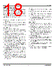
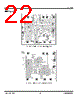
18 / 24 page  Micrel, Inc. MIC2174 September 2009 18 M9999-090409-B PCB Layout Guideline Warning!!! To minimize EMI and output noise, follow these layout recommendations. PCB Layout is critical to achieve reliable, stable and efficient performance. A ground plane is required to control EMI and minimize the inductance in power, signal and return paths. The following guidelines should be followed to insure proper operation of the MIC2174 converter. IC • Place the IC and MOSFETs close to the point of load (POL). • Use fat traces to route the input and output power lines. • Signal and power grounds should be kept separate and connected at only one location. Input Capacitor • Place the HSD input capacitor next. • Place the HSD input capacitors on the same side of the board and as close to the MOSFETs as possible. • Keep both the HSD and PGND connections short. • Place several vias to the ground plane close to the HSD input capacitor ground terminal. • Use either X7R or X5R dielectric input capacitors. Do not use Y5V or Z5U type capacitors. • Do not replace the ceramic input capacitor with any other type of capacitor. Any type of capacitor can be placed in parallel with the input capacitor. • If a Tantalum input capacitor is placed in parallel with the input capacitor, it must be recommended for switching regulator applications and the operating voltage must be derated by 50%. • In “Hot-Plug” applications, a Tantalum or Electrolytic bypass capacitor must be used to limit the over- voltage spike seen on the input supply with power is suddenly applied. • An additional Tantalum or Electrolytic bypass input capacitor of 22µF or higher is required at the input power connection. • The 1µF and 0.1µF capacitors, which connect to the VIN terminal, must be located right at the IC. The VIN terminal is very noise sensitive and placement of the capacitor is very critical. Connections must be made with wide trace. Inductor • Keep the inductor connection to the switch node (LX) short. • Do not route any digital lines underneath or close to the inductor. • Keep the switch node (LX) away from the feedback (FB) pin. • The LX pin should be connected directly to the drain of the low-side MOSFET to accurate sense the voltage across the low-side MOSFET. • To minimize noise, place a ground plane underneath the inductor. Output Capacitor • Use a wide trace to connect the output capacitor ground terminal to the input capacitor ground terminal. • Phase margin will change as the output capacitor value and ESR changes. Contact the factory if the output capacitor is different from what is shown in the BOM. • The feedback trace should be separate from the power trace and connected as close as possible to the output capacitor. Sensing a long high current load trace can degrade the DC load regulation. Schottky Diode (Optional) • Place the Schottky diode on the same side of the board as the MOSFETs and HSD input capacitor. • The connection from the Schottky diode’s Anode to the input capacitors ground terminal must be as short as possible. • The diode’s Cathode connection to the switch node (LX) must be keep as short as possible. RC Snubber • Place the RC snubber on the same side of the board and as close to the MOSFETs as possible. |
|
|
Link URL |
| Lei ha avuto il aiuto da alldatasheet? [ DONATE ] |
Di alldatasheet | Richest di pubblicita | contatti | Privacy Policy | Collegamento alla scheda tecnica | scambio Link | Ricerca produttore All Rights Reserved©Alldatasheet.com |
| Russian : Alldatasheetru.com | Korean : Alldatasheet.co.kr | Spanish : Alldatasheet.es | French : Alldatasheet.fr | Italian : Alldatasheetit.com Portuguese : Alldatasheetpt.com | Polish : Alldatasheet.pl | Vietnamese : Alldatasheet.vn Indian : Alldatasheet.in | Mexican : Alldatasheet.com.mx | British : Alldatasheet.co.uk | New Zealand : Alldatasheet.co.nz |
|
Family Site : ic2ic.com |
icmetro.com |
 Italian ▼
 English
 Chinese
 German
 Japanese
 Russian
 Korean
 Spanish
 French
 Italian
 Portuguese
 Polish
 Vietnamese
 Indian
 Mexican
 British
 New Zealand