|
Motore di ricerca datesheet componenti elettronici |
|
|
Motore di ricerca datesheet componenti elettronici |
|
MPC8378E Scheda tecnica(PDF) 39 Page - Freescale Semiconductor, Inc |
|
|
|||||||||||||||||||||||||||||
MPC8378E Scheda tecnica(HTML) 39 Page - Freescale Semiconductor, Inc |
|
|
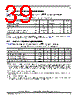
39 / 127 page  MPC8378E PowerQUICC II Pro Processor Hardware Specifications, Rev. 4 Freescale Semiconductor 39 USB 9.1 USB DC Electrical Characteristics Table 39 provides the DC electrical characteristics for the ULPI interface at recommended OVDD = 3.3 V ± 165 mV. 9.2 USB AC Electrical Specifications Table 40 describes the general timing parameters of the USB interface of the device. Table 39. USB DC Electrical Characteristics Parameter Symbol Min Max Unit Notes High-level input voltage VIH 2OVDD + 0.3 V 1 Low-level input voltage VIL –0.3 0.8 V 1 Input current IIN —±30 μA2 High-level output voltage, IOH = –100 μAVOH OVDD – 0.2 — V — Low-level output voltage, IOL = 100 μAVOL —0.2 V — Note: 1 The minimum V IL and maximum VIH values are based on the respective minimum and maximum OVIN values found in Table 3. 2 The symbol OV IN represents the input voltage of the supply and is referenced in Table 3. Table 40. USB General Timing Parameters (ULPI Mode Only) Parameter Symbol 1 Min Max Unit Notes USB clock cycle time tUSCK 15 — ns 2, 3, 4, 5 Input setup to USB clock—all inputs tUSIVKH 4 — ns 2, 3, 4, 5 Input hold to USB clock—all inputs tUSIXKH 1 — ns 2, 3, 4, 5 USB clock to output valid—all outputs tUSKHOV — 7 ns 2, 3, 4, 5 Output hold from USB clock—all outputs tUSKHOX 2 — ns 2, 3, 4, 5 Note: 1 The symbols for timing specifications follow the pattern of t (First two letters of functional block)(signal)(state) (reference)(state) for inputs and t(First two letters of functional block)(reference)(state)(signal)(state) for outputs. For example, tUSIXKH symbolizes USB timing (US) for the input (I) to go invalid (X) with respect to the time the USB clock reference (K) goes high (H). Also, tUSKHOX symbolizes USB timing (US) for the USB clock reference (K) to go high (H) with respect to the output (O) going invalid (X) or output hold time. 2 All timings are in reference to the USB clock, USBDR_CLK. 3 All signals are measured from OV DD/2 of the rising edge of the USB clock to 0.4 × OVDD of the signal in question for 3.3-V signaling levels. 4 Input timings are measured at the pin. 5 For active/float timing measurements, the high impedance or off state is defined to be when the total current delivered through the component pin is less than or equal to that of the leakage current specification. |
|
Link URL |
| Lei ha avuto il aiuto da alldatasheet? [ DONATE ] |
Di alldatasheet | Richest di pubblicita | contatti | Privacy Policy | Collegamento alla scheda tecnica | scambio Link | Ricerca produttore All Rights Reserved©Alldatasheet.com |
| Russian : Alldatasheetru.com | Korean : Alldatasheet.co.kr | Spanish : Alldatasheet.es | French : Alldatasheet.fr | Italian : Alldatasheetit.com Portuguese : Alldatasheetpt.com | Polish : Alldatasheet.pl | Vietnamese : Alldatasheet.vn Indian : Alldatasheet.in | Mexican : Alldatasheet.com.mx | British : Alldatasheet.co.uk | New Zealand : Alldatasheet.co.nz |
|
Family Site : ic2ic.com |
icmetro.com |
 Italian ▼
 English
 Chinese
 German
 Japanese
 Russian
 Korean
 Spanish
 French
 Italian
 Portuguese
 Polish
 Vietnamese
 Indian
 Mexican
 British
 New Zealand