|
Motore di ricerca datesheet componenti elettronici |
|
|
Motore di ricerca datesheet componenti elettronici |
|
PIC16F716 Scheda tecnica(PDF) 9 Page - Microchip Technology |
|
|
|||||||||||||||||||||||||||||
PIC16F716 Scheda tecnica(HTML) 9 Page - Microchip Technology |
|
|
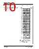
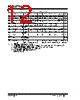
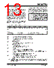
9 / 136 page  © 2007 Microchip Technology Inc. DS41206B-page 7 PIC16F716 2.0 MEMORY ORGANIZATION There are two memory blocks in the PIC16F716 device. Each block (program memory and data memory) has its own bus so that concurrent access can occur. 2.1 Program Memory Organization The PIC16F716 has a 13-bit program counter capable of addressing an 8K x 14 program memory space. The PIC16F716 has 2K x 14 words of program memory. Accessing a location above the physically implemented address will cause a wrap-around. The Reset vector is at 0000h and the interrupt vector is at 0004h. FIGURE 2-1: PROGRAM MEMORY MAP AND STACK OF PIC16F716 2.2 Data Memory Organization The data memory is partitioned into multiple banks which contain the General Purpose Registers (GPR) and the Special Function Registers (SFR). Bits RP1 and RP0 of the STATUS register are the bank select bits. Each bank extends up to 7Fh (128 bytes). The lower locations of each bank are reserved for the Special Function Registers. Above the Special Function Registers are General Purpose Registers, implemented as static RAM. All implemented banks contain Special Function Registers. The upper 16 bytes of GPR space and some “high use” Special Function Registers in Bank 0 are mirrored in Bank 1 for code reduction and quicker access. PC<12:0> 13 0000h 0004h 0005h 07FFh 0800h 1FFFh Stack Level 1 Stack Level 8 Reset Vector Interrupt Vector On-chip Program Memory CALL, RETURN RETFIE, RETLW RP<1:0>(1) (Status<6:5>) Bank 00 0 01 1 10 2(2) 11 3(2) Note 1: Maintain Status bit 6 clear to ensure upward compatibility with future products. 2: Not implemented |
|
Link URL |
| Lei ha avuto il aiuto da alldatasheet? [ DONATE ] |
Di alldatasheet | Richest di pubblicita | contatti | Privacy Policy | Collegamento alla scheda tecnica | scambio Link | Ricerca produttore All Rights Reserved©Alldatasheet.com |
| Russian : Alldatasheetru.com | Korean : Alldatasheet.co.kr | Spanish : Alldatasheet.es | French : Alldatasheet.fr | Italian : Alldatasheetit.com Portuguese : Alldatasheetpt.com | Polish : Alldatasheet.pl | Vietnamese : Alldatasheet.vn Indian : Alldatasheet.in | Mexican : Alldatasheet.com.mx | British : Alldatasheet.co.uk | New Zealand : Alldatasheet.co.nz |
|
Family Site : ic2ic.com |
icmetro.com |
 Italian ▼
 English
 Chinese
 German
 Japanese
 Russian
 Korean
 Spanish
 French
 Italian
 Portuguese
 Polish
 Vietnamese
 Indian
 Mexican
 British
 New Zealand