|
Motore di ricerca datesheet componenti elettronici |
|
|
Motore di ricerca datesheet componenti elettronici |
|
PIC16F716 Scheda tecnica(PDF) 11 Page - Microchip Technology |
|
|
|||||||||||||||||||||||||||||
PIC16F716 Scheda tecnica(HTML) 11 Page - Microchip Technology |
|
|
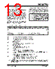
11 / 136 page  © 2007 Microchip Technology Inc. DS41206B-page 9 PIC16F716 2.2.2 SPECIAL FUNCTION REGISTERS The Special Function Registers are registers used by the CPU and peripheral modules for controlling the desired operation of the device. These registers are implemented as static RAM. A list of these registers is give in Table 2-1. The Special Function Registers can be classified into two sets; core (CPU) and peripheral. Those registers associated with the core functions are described in detail in this section. Those related to the operation of the peripheral features are described in detail in that peripheral feature section. TABLE 2-1: SPECIAL FUNCTION REGISTER SUMMARY BANK 0 Address Name Bit 7 Bit 6 Bit 5 Bit 4 Bit 3 Bit 2 Bit 1 Bit 0 Value on POR, BOR Page 00h INDF(1) Addressing this location uses contents of FSR to address data memory (not a physical register) 0000 0000 18 01h TMR0 Timer0 module’s register xxxx xxxx 27 02h PCL(1) Program Counter’s (PC) Least Significant Byte 0000 0000 17 03h STATUS(1) IRP(4) RP1(4) RP0 TO PD ZDC C 0001 1xxx 11 04h FSR(1) Indirect Data Memory Address Pointer xxxx xxxx 18 05h PORTA(5,6) — — —(7) RA4 RA3 RA2 RA1 RA0 ---x 0000 19 06h PORTB(5,6) RB7 RB6 RB5 RB4 RB3 RB2 RB1 RB0 xxxx xxxx 21 07h-09h — Unimplemented — 0Ah PCLATH(1,2) — — — Write Buffer for the upper 5 bits of the Program Counter ---0 0000 17 0Bh INTCON(1) GIE PEIE T0IE INTE RBIE T0IF INTF RBIF 0000 000x 13 0Ch PIR1 —ADIF — — — CCP1IF TMR2IF TMR1IF -0-- -000 15 0Dh — Unimplemented — 0Eh TMR1L Holding Register for the Least Significant Byte of the 16-bit TMR1 Register xxxx xxxx 29 0Fh TMR1H Holding Register for the Most Significant Byte of the 16-bit TMR1 Register xxxx xxxx 29 10h T1CON — — T1CKPS1 T1CKPS0 T1OSCEN T1SYNC TMR1CS TMR1ON --00 0000 32 11h TMR2 Timer2 Module’s Register 0000 0000 35 12h T2CON — TOUTPS3 TOUTPS2 TOUTPS1 TOUTPS0 TMR2ON T2CKPS1 T2CKPS0 -000 0000 36 13h-14h — Unimplemented — 15h CCPR1L Capture/Compare/PWM Register 1 (LSB) xxxx xxxx 48 16h CCPR1H Capture/Compare/PWM Register 1 (MSB) xxxx xxxx 48 17h CCP1CON P1M1 P1M0 DC1B1 DC1B0 CCP1M3 CCP1M2 CCP1M1 CCP1M0 0000 0000 48 18h PWM1CON PRSEN PDC6 PDC5 PDC4 PDC3 PDC2 PDC1 PDC0 0000 0000 60 19h ECCPAS ECCPASE ECCPAS2 —(8) ECCPAS0 PSSAC1 PSSAC0 PSSBD1 PSSBD0 00-0 0000 57 1Ah-1Dh — Unimplemented — 1Eh ADRES A/D Result Register xxxx xxxx 37 1Fh ADCON0 ADCS1 ADCS0 CHS2 CHS1 CHS0 GO/DONE —(7) ADON 0000 0000 41 Legend: x = unknown, u = unchanged, q = value depends on condition, – = unimplemented, read as ‘0’, Shaded locations are unimplemented, read as ‘0’. Note 1: These registers can be addressed from either bank. 2: The upper byte of the program counter is not directly accessible. PCLATH is a holding register for PC<12:8> whose contents are transferred to the upper byte of the program counter. 3: Other (non Power-up) Resets include: external Reset through MCLR and the Watchdog Timer Reset. 4: The IRP and RP1 bits are reserved. Always maintain these bits clear. 5: On any device Reset, these pins are configured as inputs. 6: This is the value that will be in the PORT output latch. 7: Reserved bits, do not use. 8: ECCPAS1 bit is not used on PIC16F716. |
|
Link URL |
| Lei ha avuto il aiuto da alldatasheet? [ DONATE ] |
Di alldatasheet | Richest di pubblicita | contatti | Privacy Policy | Collegamento alla scheda tecnica | scambio Link | Ricerca produttore All Rights Reserved©Alldatasheet.com |
| Russian : Alldatasheetru.com | Korean : Alldatasheet.co.kr | Spanish : Alldatasheet.es | French : Alldatasheet.fr | Italian : Alldatasheetit.com Portuguese : Alldatasheetpt.com | Polish : Alldatasheet.pl | Vietnamese : Alldatasheet.vn Indian : Alldatasheet.in | Mexican : Alldatasheet.com.mx | British : Alldatasheet.co.uk | New Zealand : Alldatasheet.co.nz |
|
Family Site : ic2ic.com |
icmetro.com |
 Italian ▼
 English
 Chinese
 German
 Japanese
 Russian
 Korean
 Spanish
 French
 Italian
 Portuguese
 Polish
 Vietnamese
 Indian
 Mexican
 British
 New Zealand