|
Motore di ricerca datesheet componenti elettronici |
|
|
Motore di ricerca datesheet componenti elettronici |
|
MAX7300AGL Scheda tecnica(PDF) 6 Page - Maxim Integrated Products |
|
|
|||||||||||||||||||||||||||||
MAX7300AGL Scheda tecnica(HTML) 6 Page - Maxim Integrated Products |
|
|
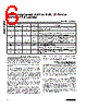
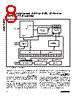
6 / 22 page  2-Wire-Interfaced, 2.5V to 5.5V, 20-Port or 28-Port I/O Expander 6 _______________________________________________________________________________________ Detailed Description The MAX7300 general-purpose input/output (GPIO) peripheral provides up to 28 I/O ports, P4 to P31, con- trolled through an I 2C-compatible serial interface. The ports can be configured to any combination of logic inputs and logic outputs, and default to logic inputs on power-up. Figure 1 is the MAX7300 functional diagram. Any I/O port can be configured as a push-pull output (sinking 10mA, sourcing 4.5mA), or a Schmitt-trigger logic input. Each input has an individually selectable internal pullup resis- tor. Additionally, transition detection allows seven ports (P24 to P30) to be monitored in any maskable combina- tion for changes in their logic status. A detected transi- tion is flagged through a status register bit, as well as an interrupt pin (port P31), if desired. The port configuration registers individually set the 28 ports, P4 to P31, as GPIO. A pair of bits in registers 0x09 through 0x0F sets each port’s configuration (Tables 1 and 2). The 36-pin MAX7300AAX and 40-pin MAX7300AGL have 28 ports, P4 to P31. The 28-pin MAX7300ANI and MAX7300AAI have only 20 ports available, P12 to P31. The eight unused ports should be configured as out- puts on power-up by writing 0x55 to registers 0x09 and 0x0A. If this is not done, the eight unused ports remain as floating inputs and quiescent supply current rises, although there is no damage to the part. Register Control of I/O Ports Across Multiple Drivers The MAX7300 offers 20 or 28 I/O ports, depending on package choice. Two addressing methods are avail- able. Any single port (bit) can be written (set/cleared) at once; or, any sequence of eight ports can be written (set/cleared) in any combination at once. There are no boundaries; it is equally acceptable to write P0 to P7, P1 to P8, or P31 to P38 (P32 to P38 are nonexistent, so the instructions to these bits are ignored). Shutdown When the MAX7300 is in shutdown mode, all ports are forced to inputs, and the pullup current sources are turned off. Data in the port and control registers remain unaltered, so port configuration and output levels are restored when the MAX7300 is taken out of shutdown. The MAX7300 can still be programmed while in shut- down mode. For minimum supply current in shutdown mode, logic inputs should be at GND or V+ potential. Shutdown mode is exited by setting the S bit in the con- figuration register (Table 8). PIN SSOP/DIP SSOP QFN NAME FUNCTION 1 1 36 ISET Bias Current Setting. Connect ISET to GND through a resistor (RISET) value of 39k Ω to 120kΩ. 2, 3 2, 3 37, 38, 39 GND Ground 4 4 40 AD0 Address Input 0. Sets device slave address. Connect to either GND, V+, SCL, SDA to give four logic combinations. See Table 3. 5–24 —— P12–P31 I/O Ports. P12 to P31 can be configured as push-pull outputs, CMOS- logic inputs, or CMOS-logic inputs with weak pullup resistor. — 5–32 1–10, 12–19, 21–30 P4–P31 I/O Ports. P4 to P31 can be configured as push-pull outputs, CMOS- logic inputs, or CMOS-logic inputs with weak pullup resistor. 25 33 32 SDA I 2C-Compatible Serial Data I/O 26 34 33 SCL I 2C-Compatible Serial Clock Input 27 35 34 AD1 Address Input 1. Sets device slave address. Connect to either GND, V+, SCL, SDA to give four logic combinations. See Table 3. 28 36 35 V+ Positive Supply Voltage. Bypass V+ to GND with minimum 0.047µF capacitor. Pin Description |
|
|
Link URL |
| Lei ha avuto il aiuto da alldatasheet? [ DONATE ] |
Di alldatasheet | Richest di pubblicita | contatti | Privacy Policy | Collegamento alla scheda tecnica | scambio Link | Ricerca produttore All Rights Reserved©Alldatasheet.com |
| Russian : Alldatasheetru.com | Korean : Alldatasheet.co.kr | Spanish : Alldatasheet.es | French : Alldatasheet.fr | Italian : Alldatasheetit.com Portuguese : Alldatasheetpt.com | Polish : Alldatasheet.pl | Vietnamese : Alldatasheet.vn Indian : Alldatasheet.in | Mexican : Alldatasheet.com.mx | British : Alldatasheet.co.uk | New Zealand : Alldatasheet.co.nz |
|
Family Site : ic2ic.com |
icmetro.com |
 Italian ▼
 English
 Chinese
 German
 Japanese
 Russian
 Korean
 Spanish
 French
 Italian
 Portuguese
 Polish
 Vietnamese
 Indian
 Mexican
 British
 New Zealand