|
Motore di ricerca datesheet componenti elettronici |
|
|
Motore di ricerca datesheet componenti elettronici |
|
MAX7300AGL Scheda tecnica(PDF) 7 Page - Maxim Integrated Products |
|
|
|||||||||||||||||||||||||||||
MAX7300AGL Scheda tecnica(HTML) 7 Page - Maxim Integrated Products |
|
|
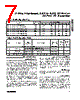
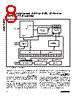
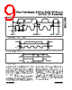
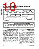
7 / 22 page  2-Wire-Interfaced, 2.5V to 5.5V, 20-Port or 28-Port I/O Expander _______________________________________________________________________________________ 7 Serial Interface Serial Addressing The MAX7300 operates as a slave that sends and receives data through an I 2C-compatible 2-wire inter- face. The interface uses a serial data line (SDA) and a serial clock line (SCL) to achieve bidirectional commu- nication between master(s) and slave(s). A master (typ- ically a microcontroller) initiates all data transfers to and from the MAX7300, and generates the SCL clock that synchronizes the data transfer (Figure 2). The MAX7300 SDA line operates as both an input and an open-drain output. A pullup resistor, typically 4.7k Ω, is required on SDA. The MAX7300 SCL line operates only as an input. A pullup resistor, typically 4.7k Ω, is required on SCL if there are multiple masters on the 2- wire interface, or if the master in a single-master system has an open-drain SCL output. Each transmission consists of a START condition (Figure 3) sent by a master, followed by the MAX7300 7-bit slave address plus R/ W bit (Figure 6), a register address byte, one or more data bytes, and finally a STOP condition (Figure 3). Start and Stop Conditions Both SCL and SDA remain high when the interface is not busy. A master signals the beginning of a transmis- sion with a START (S) condition by transitioning SDA from high to low while SCL is high. When the master has finished communicating with the slave, it issues a STOP (P) condition by transitioning SDA from low to high while SCL is high. The bus is then free for another transmission (Figure 3). Bit Transfer One data bit is transferred during each clock pulse. The data on SDA must remain stable while SCL is high (Figure 4). Acknowledge The acknowledge bit is a clocked 9th bit, which the recipient uses to handshake receipt of each byte of data (Figure 5). Thus, each byte transferred effectively requires 9 bits. The master generates the 9th clock pulse, and the recipient pulls down SDA during the acknowledge clock pulse, such that the SDA line is sta- ble low during the high period of the clock pulse. When the master is transmitting to the MAX7300, the MAX7300 generates the acknowledge bit since the Table 1. Port Configuration Map REGISTER DATA REGISTER ADDRESS CODE (HEX) D7 D6 D5 D4 D3 D2 D1 D0 Port Configuration for P7, P6, P5, P4 0x09 P7 P6 P5 P4 Port Configuration for P11, P10, P9, P8 0x0A P11 P10 P9 P8 Port Configuration for P15, P14, P13, P12 0x0B P15 P14 P13 P12 Port Configuration for P19, P18, P17, P16 0x0C P19 P18 P17 P16 Port Configuration for P23, P22, P21, P20 0x0D P23 P22 P21 P20 Port Configuration for P27, P26, P25, P24 0x0E P27 P26 P25 P24 Port Configuration for P31, P30, P29, P28 0x0F P31 P30 P29 P28 Table 2. Port Configuration Matrix PORT CONFIGURATION BIT PAIR MODE FUNCTION PORT REGISTER PIN BEHAVIOR ADDRESS CODE (HEX) UPPER LOWER DO NOT USE THIS SETTING 0x09 to 0x0F 0 0 Written Low Active-low logic output Output GPIO Output Written High Active-high logic output 0x09 to 0x0F 0 1 Input GPIO Input without Pullup Reading Port Schmitt logic output 0x09 to 0x0F 1 0 Input GPIO Input with Pullup Reading Port Schmitt logic input with pullup 0x09 to 0x0F 1 1 |
|
|
Link URL |
| Lei ha avuto il aiuto da alldatasheet? [ DONATE ] |
Di alldatasheet | Richest di pubblicita | contatti | Privacy Policy | Collegamento alla scheda tecnica | scambio Link | Ricerca produttore All Rights Reserved©Alldatasheet.com |
| Russian : Alldatasheetru.com | Korean : Alldatasheet.co.kr | Spanish : Alldatasheet.es | French : Alldatasheet.fr | Italian : Alldatasheetit.com Portuguese : Alldatasheetpt.com | Polish : Alldatasheet.pl | Vietnamese : Alldatasheet.vn Indian : Alldatasheet.in | Mexican : Alldatasheet.com.mx | British : Alldatasheet.co.uk | New Zealand : Alldatasheet.co.nz |
|
Family Site : ic2ic.com |
icmetro.com |
 Italian ▼
 English
 Chinese
 German
 Japanese
 Russian
 Korean
 Spanish
 French
 Italian
 Portuguese
 Polish
 Vietnamese
 Indian
 Mexican
 British
 New Zealand