|
Motore di ricerca datesheet componenti elettronici |
|
|
Motore di ricerca datesheet componenti elettronici |
|
HM25Q40C Scheda tecnica(PDF) 9 Page - Shenzhen Huazhimei Semiconductor Co., Ltd |
|
|
|||||||||||||||||||||||||||||
HM25Q40C Scheda tecnica(HTML) 9 Page - Shenzhen Huazhimei Semiconductor Co., Ltd |
|
|
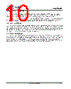
9 / 62 page  Preliminary Datasheet 9 4. SIGNAL DESCRIPTIONS Table 4.1 Pin Descriptions Symbol Pin Name CLK Serial Clock Input DI(IO0) Serial Data Input(Data input output 0) (1) DO(IO1) Serial Data Output(Data input output 1) (1) CS# Chip Enable WP#(IO2)(3) Write Protect (Data input output 2) (2) HOLD# / RESET#(3)(IO3) Hold or Reset input(Data input output 3) (2) VCC Power Supply (2.3-3.6V) GND Ground Notes: (1)IO0 and IO1 are used for Standard and Dual SPI instructions. (2)IO0—IO3 are used for QUAD SPI instructions. (3)WP# and HOLD# / RESET# functions are only available for Standard and Dual SPI. 4.1. Serial Data Input (DI) / IO0 The SPI Serial Data Input (DI) pin is used to transfer data serially into the device. It receives instructions, address and data to be programmed. Data is latched on the rising edge of the Serial Clock (CLK) input pin. The DI pin becomes IO0 - an input and output during Dual and Quad commands for receiving instructions, address, and data to be programmed (values latched on rising edge of serial CLK clock signal) as well as shifting out data (on the falling edge of CLK). 4.2. Serial Data Output (DO) / IO1 The SPI Serial Data Output (DO) pin is used to transfer data serially out of the device. Data is shifted out on the falling edge of the Serial Clock (CLK) input pin. DO becomes IO1 - an input and output during Dual and Quad commands for receiving instructions, addresses, and data to be programmed (values latched on rising edge of serial CLK clock signal) as well as shifting out data (on the falling edge of CLK). 4.3. Serial Clock (CLK) The SPI Serial Clock Input (CLK) pin provides the timing for serial input and output operations. ("See SPI Mode") 4.4. Chip Select (CS#) The SPI Chip Select (CS#) pin enables and disables device operation. When CS# is high the device is deselected and the Serial Data Output pins are at high impedance. When deselected, the devices power consumption will be at standby levels unless an internal erase, program or status register cycle is in progress. When CS# is brought low the device will be selected, power consumption will increase to active levels and instructions can be written to and data read from the device. After power-up, CS# must transition from high to low before a new instruction will be accepted. HM25Q40A |
|
Link URL |
| Lei ha avuto il aiuto da alldatasheet? [ DONATE ] |
Di alldatasheet | Richest di pubblicita | contatti | Privacy Policy | Collegamento alla scheda tecnica | scambio Link | Ricerca produttore All Rights Reserved©Alldatasheet.com |
| Russian : Alldatasheetru.com | Korean : Alldatasheet.co.kr | Spanish : Alldatasheet.es | French : Alldatasheet.fr | Italian : Alldatasheetit.com Portuguese : Alldatasheetpt.com | Polish : Alldatasheet.pl | Vietnamese : Alldatasheet.vn Indian : Alldatasheet.in | Mexican : Alldatasheet.com.mx | British : Alldatasheet.co.uk | New Zealand : Alldatasheet.co.nz |
|
Family Site : ic2ic.com |
icmetro.com |
 Italian ▼
 English
 Chinese
 German
 Japanese
 Russian
 Korean
 Spanish
 French
 Italian
 Portuguese
 Polish
 Vietnamese
 Indian
 Mexican
 British
 New Zealand