|
Motore di ricerca datesheet componenti elettronici |
|
|
Motore di ricerca datesheet componenti elettronici |
|
AD9753AST Scheda tecnica(PDF) 15 Page - Analog Devices |
|
|
|||||||||||||||||||||||||||||
AD9753AST Scheda tecnica(HTML) 15 Page - Analog Devices |
|
|
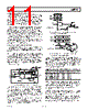
15 / 28 page  REV. B AD9753 –15– DVDD DIGITAL INPUT Figure 14. Equivalent Digital Input The AD9753 features a flexible differential clock input operat- ing from separate supplies (i.e., CLKVDD, CLKCOM) to achieve optimum jitter performance. The two clock inputs, CLK+ and CLK–, can be driven from a single-ended or differ- ential clock source. For single-ended operation, CLK+ should be driven by a logic source while CLK– should be set to the threshold voltage of the logic source. This can be done via a resistor divider/capacitor network, as shown in Figure 15a. For differential operation, both CLK+ and CLK– should be biased to CLKVDD/2 via a resistor divider network, as shown in Figure 15b. RSERIES 0.1 F VTHRESHOLD CLK+ CLKVDD CLK– CLKCOM AD9753 Figure 15a. Single-Ended Clock Interface 0.1 F CLK+ CLKVDD CLK– CLKCOM AD9753 0.1 F 0.1 F Figure 15b. Differential Clock Interface Because the output of the AD9753 can be updated at up to 300 MSPS, the quality of the clock and data input signals is important in achieving the optimum performance. The drivers of the digital data interface circuitry should be specified to meet the minimum setup-and-hold times of the AD9753 as well as its required min/max input logic level thresholds. Digital signal paths should be kept short and run lengths matched to avoid propagation delay mismatch. Inserting a low value resis- tor network (i.e., 20 Ω to 100 Ω) between the AD9753 digital inputs and driver outputs may be helpful in reducing any over- shooting and ringing at the digital inputs that contribute to data feedthrough. For longer run lengths and high data update rates, strip line techniques with proper termination resistors should be considered to maintain “clean” digital inputs. The external clock driver circuitry should provide the AD9753 with a low jitter clock input meeting the min/max logic levels while providing fast edges. Fast clock edges help minimize any jitter that will manifest itself as phase noise on a reconstructed waveform. Thus, the clock input should be driven by the fastest logic family suitable for the application. Note that the clock input could also be driven via a sine wave that is centered around the digital threshold (i.e., DVDD/2) and meets the min/max logic threshold. This typically results in a slight degradation in the phase noise, which becomes more noticeable at higher sampling rates and output frequencies. Also, at higher sampling rates, the 20% tolerance of the digital logic threshold should be considered since it will affect the effective clock duty cycle and, subsequently, cut into the required data setup-and-hold times. INPUT CLOCK AND DATA TIMING RELATIONSHIP SNR in a DAC is dependent on the relationship between the position of the clock edges and the point in time at which the input data changes. The AD9753 is rising edge triggered, and so exhibits SNR sensitivity when the data transition is close to this edge. In general, the goal when applying the AD9753 is to make the data transition close to the falling clock edge. This becomes more important as the sample rate increases. Figure 16 shows the relationship of SNR to clock placement with different sample rates. Note that the setup-and-hold times implied in Figure 16 appear to violate the maximums stated in the Digital Specifications of this data sheet. The variation in Figure 16 is due to the skew present between data bits inherent in the digital data generator used to perform these tests. Figure 16 is presented to show the effects of violating setup-and-hold times and to show the insensitivity of the AD9753 to clock placement when data transitions fall outside of the so-called “bad window.” The setup-and-hold times stated in the Digital Specifications table were measured on a bit-by-bit basis, therefore eliminating the skew present in the digital data generator. At higher data rates, it becomes very important to account for the skew in the input digital data when defining timing specifications. TIME OF DATA TRANSITION RELATIVE TO PLACEMENT OF CLK RISING EDGE (ns), fOUT = 10MHz, fDAC = 300MHz 80 40 0 3 0 –3 60 20 70 30 50 10 –2 –1 1 2 Figure 16. SNR vs. Time of Data Transition Relative to Clock Rising Edge POWER DISSIPATION The power dissipation, PD, of the AD9753 is dependent on several factors that include the power supply voltages (AVDD and DVDD), the full-scale current output IOUTFS, the update rate fCLOCK, and the reconstructed digital input waveform. The power dissipation is directly proportional to the analog sup- ply current, IAVDD, and the digital supply current, IDVDD. IAVDD is directly proportional to IOUTFS, as shown in Figure 17, |
|
Link URL |
| Lei ha avuto il aiuto da alldatasheet? [ DONATE ] |
Di alldatasheet | Richest di pubblicita | contatti | Privacy Policy | Collegamento alla scheda tecnica | scambio Link | Ricerca produttore All Rights Reserved©Alldatasheet.com |
| Russian : Alldatasheetru.com | Korean : Alldatasheet.co.kr | Spanish : Alldatasheet.es | French : Alldatasheet.fr | Italian : Alldatasheetit.com Portuguese : Alldatasheetpt.com | Polish : Alldatasheet.pl | Vietnamese : Alldatasheet.vn Indian : Alldatasheet.in | Mexican : Alldatasheet.com.mx | British : Alldatasheet.co.uk | New Zealand : Alldatasheet.co.nz |
|
Family Site : ic2ic.com |
icmetro.com |
 Italian ▼
 English
 Chinese
 German
 Japanese
 Russian
 Korean
 Spanish
 French
 Italian
 Portuguese
 Polish
 Vietnamese
 Indian
 Mexican
 British
 New Zealand