|
Motore di ricerca datesheet componenti elettronici |
|
|
Motore di ricerca datesheet componenti elettronici |
|
AD9753AST Scheda tecnica(PDF) 18 Page - Analog Devices |
|
|
|||||||||||||||||||||||||||||
AD9753AST Scheda tecnica(HTML) 18 Page - Analog Devices |
|
|
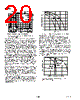
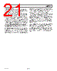
18 / 28 page  REV. B –18– AD9753 This is referred to as the Power Supply Rejection Ratio. For dc variations of the power supply, the resulting performance of the DAC directly corresponds to a gain error associated with the DAC’s full-scale current, IOUTFS. AC noise on the dc supplies is common in applications where the power distribution is gener- ated by a switching power supply. Typically, switching power supply noise will occur over the spectrum from tens of kHz to several MHz. The PSRR versus the frequency of the AD9753 AVDD supply over this frequency range is shown in Figure 25. FREQUENCY (MHz) 85 40 12 6 0 80 75 70 65 60 55 50 45 24 8 10 Figure 25. Power Supply Rejection Ratio Note that the units in Figure 25 are given in units of (amps out/ volts in). Noise on the analog power supply has the effect of modulating the internal switches, and therefore the output current. The voltage noise on AVDD will thus be added in a nonlinear manner to the desired IOUT. Due to the relative different size of these switches, PSRR is very code-dependent. This can produce a mixing effect that can modulate low fre- quency power supply noise to higher frequencies. Worst-case PSRR for either one of the differential DAC outputs will occur when the full-scale current is directed toward that output. As a result, the PSRR measurement in Figure 25 represents a worst- case condition in which the digital inputs remain static and the full-scale output current of 20 mA is directed to the DAC out- put being measured. An example serves to illustrate the effect of supply noise on the analog supply. Suppose a switching regulator with a switching frequency of 250 kHz produces 10 mV rms of noise and, for simplicity sake (i.e., ignore harmonics), all of this noise is con- centrated at 250 kHz. To calculate how much of this undesired noise will appear as current noise superimposed on the DAC’s full-scale current, IOUTFS, one must determine the PSRR in dB using Figure 25 at 250 kHz. To calculate the PSRR for a given RLOAD, such that the units of PSRR are converted from A/V to V/V, adjust the curve in Figure 25 by the scaling factor 20 × Log (RLOAD ). For instance, if RLOAD is 50 Ω, the PSRR is reduced by 34 dB, i.e., PSRR of the DAC at 250 kHz, which is 85 dB in Figure 25, becomes 51 dB VOUT/VIN. Proper grounding and decoupling should be a primary objective in any high speed, high resolution system. The AD9753 features separate analog and digital supply and ground pins to optimize the management of analog and digital ground currents in a system. In general, AVDD, the analog supply, should be decoupled to ACOM, the analog common, as close to the chip as physically possible. Similarly, DVDD, the digital supply, should be decoupled to DCOM as close to the chip as physically possible. For those applications that require a single 3.3 V supply for both the analog and digital supplies, a clean analog supply may be generated using the circuit shown in Figure 26. The circuit consists of a differential LC filter with separate power supply and return lines. Lower noise can be attained by using low ESR type electrolytic and tantalum capacitors. AVDD ACOM 100 F ELECT. 10 F TANT. 0.1 F CER. TTL/CMOS LOGIC CIRCUITS 3.3V POWER SUPPLY FERRITE BEADS Figure 26. Differential LC Filter for a Single 3.3 V Application APPLICATIONS QAM/PSK Synthesis Quadrature modulation (QAM or PSK) consists of two base- band PAM (Pulse Amplitude Modulated) data channels. Both channels are modulated by a common frequency carrier. How- ever, the carriers for each channel are phase-shifted 90 ° from each other. This orthogonality allows twice the spectral efficiency (data for a given bandwidth) of digital data transmitted via AM. Receivers can be designed to selectively choose the “in phase” and “quadrature” carriers, and then recombine the data. The recombi- nation of the QAM data can be mapped as points representing digital words in a two dimensional constellation as shown in Figure 27. Each point, or symbol, represents the transmission of multiple bits in one symbol period. 0100 0101 0001 0000 0110 0111 0011 0010 1110 1111 1011 1010 1100 1101 1001 1000 Figure 27. 16 QAM Constellation, Gray Coded (Two 4-Level PAM Signals with Orthogonal Carriers) Typically, the I and Q data channels are quadrature-modulated in the digital domain. The high data rate of the AD9753 allows extremely wideband (>10 MHz) quadrature carriers to be syn- thesized. Figure 28 shows an example of a 25 MSymbol/S QAM signal, oversampled by 8 at a data rate of 200 MSPS, modu- lated onto a 25 MHz carrier and reconstructed using the AD9753. The power in the reconstructed signal is measured to be –11.92 dBm. In the first adjacent band, the power is –76.86 dBm, while in the second adjacent band, the power is –80.96 dBm. |
|
Link URL |
| Lei ha avuto il aiuto da alldatasheet? [ DONATE ] |
Di alldatasheet | Richest di pubblicita | contatti | Privacy Policy | Collegamento alla scheda tecnica | scambio Link | Ricerca produttore All Rights Reserved©Alldatasheet.com |
| Russian : Alldatasheetru.com | Korean : Alldatasheet.co.kr | Spanish : Alldatasheet.es | French : Alldatasheet.fr | Italian : Alldatasheetit.com Portuguese : Alldatasheetpt.com | Polish : Alldatasheet.pl | Vietnamese : Alldatasheet.vn Indian : Alldatasheet.in | Mexican : Alldatasheet.com.mx | British : Alldatasheet.co.uk | New Zealand : Alldatasheet.co.nz |
|
Family Site : ic2ic.com |
icmetro.com |
 Italian ▼
 English
 Chinese
 German
 Japanese
 Russian
 Korean
 Spanish
 French
 Italian
 Portuguese
 Polish
 Vietnamese
 Indian
 Mexican
 British
 New Zealand