|
Motore di ricerca datesheet componenti elettronici |
|
|
Motore di ricerca datesheet componenti elettronici |
|
AD9753AST Scheda tecnica(PDF) 21 Page - Analog Devices |
|
|
|||||||||||||||||||||||||||||
AD9753AST Scheda tecnica(HTML) 21 Page - Analog Devices |
|
|
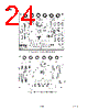
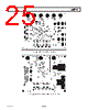
21 / 28 page  REV. B AD9753 –21– EVALUATION BOARD The AD9753-EB is an evaluation board for the AD9753 TxDAC. Careful attention to layout and circuit design, combined with prototyping area, allows the user to easily and effectively evalu- ate the AD9753 in different modes of operation. Referring to Figures 34 and 35, the AD9753’s performance can be evaluated differentially or single-ended either using a trans- former, or directly coupling the output. To evaluate the output differentially using the transformer, it is recommended that either the Mini-Circuits T1-1T (through-hole) or the Coilcraft TTWB-1-B (SMT) be placed in the position of T1 on the evalua- tion board. To evaluate the output either single-ended or direct- coupled, remove the transformer and bridge either BL1 or BL2. The digital data to the AD9753 comes from two ribbon cables that interface to the 40-lead IDC connectors P1 and P2. Proper termi- nation or voltage scaling can be accomplished by installing the resistor pack networks RN1–RN12. RN1, 4, 7, and 10 are 22 Ω DIP resistor packs and should be installed as they help reduce the digital edge rates and therefore peak current on the inputs. A single-ended clock can be applied via J3. By setting the SE/ DIFF labeled jumpers J2, 3, 4, and 6, the input clock can be directed to the CLK+/CLK– inputs of the AD9753 in either a single-ended or differential manner. If a differentially applied clock is desired, a Mini-Circuits T1-1T transformer should be used in the position of T2. Note that with a single-ended square wave clock input, T2 must be removed. A clock can also be applied via the ribbon cable on Port 1 (P1), Pin 33. By inserting the EDGE jumper (JP1), this clock will be applied to the CLK+ input of the AD9753. JP3 should be set in its SE position in this application to bias CLK– to 1/2 the supply voltage. The AD9753’s PLL clock multiplier can be enabled by inserting JP7 in the IN position. As described in the Typical Performance Characteristics and Functional Description sections, with the PLL enabled, a clock at 1/2 the output data rate should be applied as described in the last paragraph. The PLL takes care of the internal 2 × frequency multiplication and all internal timing requirements. In this application, the PLLLOCK output indicates when lock is achieved on the PLL. With the PLL enabled, the DIV0 and DIV1 jumpers (JP8 and JP9) provide the PLL divider ratio as described in Table I. The PLL is disabled when JP7 is in the EX setting. In this mode, a clock at the speed of the output data rate must be applied to the clock inputs. Internally, the clock is divided by 2. For data synchronization, a 1 clock is provided on the PLLLOCK pin in this application. Care should be taken to read the timing requirements described earlier in the data sheet for optimum performance. With the PLL disabled, the DIV0 and DIV1 jumpers define the mode (interleaved, noninterleaved) as described in Table II. |
|
Link URL |
| Lei ha avuto il aiuto da alldatasheet? [ DONATE ] |
Di alldatasheet | Richest di pubblicita | contatti | Privacy Policy | Collegamento alla scheda tecnica | scambio Link | Ricerca produttore All Rights Reserved©Alldatasheet.com |
| Russian : Alldatasheetru.com | Korean : Alldatasheet.co.kr | Spanish : Alldatasheet.es | French : Alldatasheet.fr | Italian : Alldatasheetit.com Portuguese : Alldatasheetpt.com | Polish : Alldatasheet.pl | Vietnamese : Alldatasheet.vn Indian : Alldatasheet.in | Mexican : Alldatasheet.com.mx | British : Alldatasheet.co.uk | New Zealand : Alldatasheet.co.nz |
|
Family Site : ic2ic.com |
icmetro.com |
 Italian ▼
 English
 Chinese
 German
 Japanese
 Russian
 Korean
 Spanish
 French
 Italian
 Portuguese
 Polish
 Vietnamese
 Indian
 Mexican
 British
 New Zealand