|
Motore di ricerca datesheet componenti elettronici |
|
|
Motore di ricerca datesheet componenti elettronici |
|
AS5047D Scheda tecnica(PDF) 9 Page - ams AG |
|
|
|||||||||||||||||||||||||||||
AS5047D Scheda tecnica(HTML) 9 Page - ams AG |
|
|
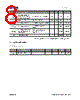
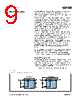
9 / 37 page  ams Datasheet: 2014-Jun-27 [v1-02] AS5047D – 9 Detaile d Desc rip t ion The AS5047D is a Hall-effect magnetic sensor using a CMOS lateral technology. The lateral Hall sensors convert the magnetic field component perpendicular to the surface of the chip into a voltage. The signals from the Hall sensors are amplified and filtered by the analog front-end (AFE) before being converted by the analog-to-digital converter (ADC). The output of the ADC is processed by the hardwired CORDIC (coordinate rotating digital computer) block to compute the angle and magnitude of the magnetic vector. The intensity of the magnetic field (magnitude) is used by the automatic gain control (AGC) to adjust the amplification level for compensation of the temperature and magnetic field variations. The internal 14-bit resolution is available by reading a register through the SPI interface. The resolution on the ABI output can be programmed from 2048 to 32 steps per revolution. The Dynamic Angle Error Compensation block corrects the calculated angle for latency using a linear prediction calculation algorithm. At constant rotation speed the latency time is internally compensated by the AS5047D, reducing the dynamic angle error at the SPI, ABI and UVW outputs. The AS5047D allows to switch off the UVW output interface to display the absolute angle as PWM-encoded signal on the pin W. At higher speeds, the interpolator fills in missing ABI pulses and generates the UVW signals with no loss of resolution. The non-volatile settings in the AS5047D can be programmed through the SPI interface without any dedicated programmer. Power Management The AS5047D can be either powered from a 5.0V supply using the on-chip low-dropout regulator or from a 3.3V voltage supply. The LDO regulator is not intended to power any other loads, and it needs a 1 μF capacitor to ground located close to the chip for decoupling as shown in Figure 10. In 3.3V operation, VDD and VREG must be tied together. Figure 10: 5.0V and 3.3V Power Supply Options Detailed Description 1µF 100nF 4.5 - 5.5V VDD3V3 GND VDD 5.0V Operation LDO AS5047D 100nF 3.0 – 3.6V VDD3V3 GND VDD 3.3V Operation LDO AS5047D |
|
Link URL |
| Lei ha avuto il aiuto da alldatasheet? [ DONATE ] |
Di alldatasheet | Richest di pubblicita | contatti | Privacy Policy | Collegamento alla scheda tecnica | scambio Link | Ricerca produttore All Rights Reserved©Alldatasheet.com |
| Russian : Alldatasheetru.com | Korean : Alldatasheet.co.kr | Spanish : Alldatasheet.es | French : Alldatasheet.fr | Italian : Alldatasheetit.com Portuguese : Alldatasheetpt.com | Polish : Alldatasheet.pl | Vietnamese : Alldatasheet.vn Indian : Alldatasheet.in | Mexican : Alldatasheet.com.mx | British : Alldatasheet.co.uk | New Zealand : Alldatasheet.co.nz |
|
Family Site : ic2ic.com |
icmetro.com |
 Italian ▼
 English
 Chinese
 German
 Japanese
 Russian
 Korean
 Spanish
 French
 Italian
 Portuguese
 Polish
 Vietnamese
 Indian
 Mexican
 British
 New Zealand