|
Motore di ricerca datesheet componenti elettronici |
|
|
Motore di ricerca datesheet componenti elettronici |
|
TDA4VEN...Q1 Scheda tecnica(PDF) 50 Page - Texas Instruments |
|
|
|||||||||||||||||||||||||||||
TDA4VEN...Q1 Scheda tecnica(HTML) 50 Page - Texas Instruments |
|
|
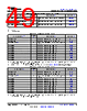
50 / 236 page  Table 5-9. CSIRX2 Signal Descriptions SIGNAL NAME [1] PIN TYPE [2] DESCRIPTION [3] AMW PIN [4] CSI2_RXCLKN I CSI Differential Receive Clock Input (negative) AG8 CSI2_RXCLKP I CSI Differential Receive Clock Input (positive) AG9 CSI2_RXRCALIB (1) A CSI pin connected to external resistor for on-chip resistor calibration AB14 CSI2_RXN0 I CSI Differential Receive Input (negative) AF9 CSI2_RXN1 I CSI Differential Receive Input (negative) AE10 CSI2_RXN2 I CSI Differential Receive Input (negative) AD11 CSI2_RXN3 I CSI Differential Receive Input (negative) AC13 CSI2_RXP0 I CSI Differential Receive Input (positive) AF10 CSI2_RXP1 I CSI Differential Receive Input (positive) AE11 CSI2_RXP2 I CSI Differential Receive Input (positive) AD12 CSI2_RXP3 I CSI Differential Receive Input (positive) AC12 (1) An external 499 Ω ±1% resistor must be connected between this pin and VSS and the maximum power dissipation for the resistor is 7.2mW. No external voltage should be applied to this pin. Table 5-10. CSIRX3 Signal Descriptions SIGNAL NAME [1] PIN TYPE [2] DESCRIPTION [3] AMW PIN [4] CSI3_RXCLKN I CSI Differential Receive Clock Input (negative) AG12 CSI3_RXCLKP I CSI Differential Receive Clock Input (positive) AG11 CSI3_RXRCALIB (1) A CSI pin connected to external resistor for on-chip resistor calibration AB15 CSI3_RXN0 I CSI Differential Receive Input (negative) AF13 CSI3_RXN1 I CSI Differential Receive Input (negative) AE14 CSI3_RXN2 I CSI Differential Receive Input (negative) AD15 CSI3_RXN3 I CSI Differential Receive Input (negative) AC15 CSI3_RXP0 I CSI Differential Receive Input (positive) AF12 CSI3_RXP1 I CSI Differential Receive Input (positive) AE13 CSI3_RXP2 I CSI Differential Receive Input (positive) AD14 CSI3_RXP3 I CSI Differential Receive Input (positive) AC16 (1) An external 499 Ω ±1% resistor must be connected between this pin and VSS and the maximum power dissipation for the resistor is 7.2mW. No external voltage should be applied to this pin. 5.3.4 DDRSS 5.3.4.1 MAIN Domain Table 5-11. DDRSS0 Signal Descriptions SIGNAL NAME [1] PIN TYPE [2] DESCRIPTION [3] AMW PIN [4] DDR0_CAS_n (1) O DDRSS Column Address Strobe / LPDDR4 Chip Select 1B M4 DDR0_RAS_n (1) O DDRSS Row Address Strobe / LPDDR4 Chip Select 0B M3 DDR0_A0 O DDRSS Address Bus L4 DDR0_A1 O DDRSS Address Bus L6 DDR0_A2 O DDRSS Address Bus M5 DDR0_A3 O DDRSS Address Bus L3 DDR0_A4 O DDRSS Address Bus N2 DDR0_A5 O DDRSS Address Bus L2 DDR0_CAL0 (2) A IO Pad Calibration Resistor R6 TDA4VEN-Q1, TDA4AEN-Q1 SPRSP96A – MARCH 2024 – REVISED SEPTEMBER 2024 www.ti.com 50 Submit Document Feedback Copyright © 2024 Texas Instruments Incorporated Product Folder Links: TDA4VEN-Q1 TDA4AEN-Q1 |
|
Link URL |
| Lei ha avuto il aiuto da alldatasheet? [ DONATE ] |
Di alldatasheet | Richest di pubblicita | contatti | Privacy Policy | Collegamento alla scheda tecnica | scambio Link | Ricerca produttore All Rights Reserved©Alldatasheet.com |
| Russian : Alldatasheetru.com | Korean : Alldatasheet.co.kr | Spanish : Alldatasheet.es | French : Alldatasheet.fr | Italian : Alldatasheetit.com Portuguese : Alldatasheetpt.com | Polish : Alldatasheet.pl | Vietnamese : Alldatasheet.vn Indian : Alldatasheet.in | Mexican : Alldatasheet.com.mx | British : Alldatasheet.co.uk | New Zealand : Alldatasheet.co.nz |
|
Family Site : ic2ic.com |
icmetro.com |
 Italian ▼
 English
 Chinese
 German
 Japanese
 Russian
 Korean
 Spanish
 French
 Italian
 Portuguese
 Polish
 Vietnamese
 Indian
 Mexican
 British
 New Zealand