|
Motore di ricerca datesheet componenti elettronici |
|
|
Motore di ricerca datesheet componenti elettronici |
|
RC19302A00AGNT#BD0 Scheda tecnica(PDF) 39 Page - Renesas Technology Corp |
|
|
|||||||||||||||||||||||||||||
RC19302A00AGNT#BD0 Scheda tecnica(HTML) 39 Page - Renesas Technology Corp |
|
|
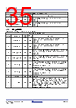
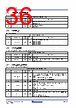
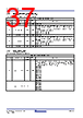
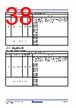
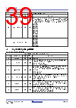
39 / 62 page  R31DS0210EU0106 Rev.1.06 Page 39 May 11, 2026 RC193xx Datasheet 4.5.11 PD_RESTORE_LOSb_CONFIG Configuration and Status Register. 3:0 amp_cntrl_def_bnk0 RW 0x7 Default amplitude control for bank 0. When the multifunction pin is configured as Amplitude Select, this field defines the single-ended output amplitude of the Bank 0 (CLK[3:0]) when the pin = 0. When the multifunction pin is configured as Slew Rate Selection, this field determines the amplitude of bank 0 (CLK[3:0]). 0x0 = 625mV 0x1 = 650mV 0x2 = 675mV 0x3 = 700mV 0x4 = 725mV 0x5 = 750mV 0x6 = 775mV 0x7 = 800mV 0x8 = 825mV 0x9 = 850mV amp_cntrl_def_bnk0 (continued) 0xA = 875mV 0xB = 900mV 0xC = 925mV 0xD = 950mV 0xE = 975mV 0xF = 1000mV PD_RESTORE_LOSb_CONFIG Bit Field Descriptions Bit Field Field Name Field Type Default Value Description 7:5 reserved RW 0x0 Reserved 4 ck_acquire_rb RO 0x0 Clock acquired read-back. This bit indicates if a clock was ever detected (LOSb de-asserted) for the current power cycle. 0 = Clock never acquired 1 = Clock acquired once before 3 pd_restoreb RW 0x1 Save configuration in power-down. This bit determines the behavior of the device when the PWRGD_PWRDNb pin is asserted low. This bit is automatically returned to 1 after PWRGD_PWRDNb is toggled 1-0-1 with the bit set to 0. 0 = Config Cleared 1 = Config Saved 2 sdata_time_out_enable RW 0x1 Enable SMB time out monitoring SDATA. This bit enables a timeout for the SMBus data path. This timeout monitor is in addition to the mandatory SCLK timeout monitor. These monitors release a hung SMBus. 0 = Disable SDATA time out 1 = Enable SDATA time out 1 los1b_rb RO 0x0 Real-time read back of CLKIN1 clock detect. This bit provides a real-time status of the CLKIN1 input. The default value assumes CLKIN1 is not present. 0 = LOS event detected (no CLKIN1 detected) 1 = No LOS event detected (CLKIN1 detected) 0 los0b_rb RO 0x0 Real-time read back of CLKIN0 clock detect. This bit provides a real-time status of the CLKIN0 input. The default value assumes CLKIN0 is not present. 0 = LOS event detected (no CLKIN0 detected) 1 = No LOS event detected (CLKIN0 detected) AMP_CTRL_DEF Bit Field Descriptions Bit Field Field Name Field Type Default Value Description |
|
Link URL |
| Lei ha avuto il aiuto da alldatasheet? [ DONATE ] |
Di alldatasheet | Richest di pubblicita | contatti | Privacy Policy | Collegamento alla scheda tecnica | scambio Link | Ricerca produttore All Rights Reserved©Alldatasheet.com |
| Russian : Alldatasheetru.com | Korean : Alldatasheet.co.kr | Spanish : Alldatasheet.es | French : Alldatasheet.fr | Italian : Alldatasheetit.com Portuguese : Alldatasheetpt.com | Polish : Alldatasheet.pl | Vietnamese : Alldatasheet.vn Indian : Alldatasheet.in | Mexican : Alldatasheet.com.mx | British : Alldatasheet.co.uk | New Zealand : Alldatasheet.co.nz |
|
Family Site : ic2ic.com |
icmetro.com |
 Italian ▼
 English
 Chinese
 German
 Japanese
 Russian
 Korean
 Spanish
 French
 Italian
 Portuguese
 Polish
 Vietnamese
 Indian
 Mexican
 British
 New Zealand