 |
Motore di ricerca datesheet componenti elettronici |
|
|
Motore di ricerca datesheet componenti elettronici |
|
The question interval is too short.
Please try again in a few seconds.

Hello, Please ask a question about HYB18T512400B Datasheet
# Example questions:
➢ Compare and contrast how data strobes (dqs/udqs/ldqs) are handled in the x4/x8 configurations versus the x16 configuration based on the provided documentation.
➢ What power supply rail (e.g., vddq) is used to power the i/o drivers, and which pins are connected to it?
➢ What is the function of the 'ap' signal when connected to address line a10 in the x4/x8 configurations?
| Part No. | HYB18T512400B |
| Manufacturer | QIMONDA |
| Size | 3Mb |
| Pages | 68 pages |
| Description | 512-Mbit Double-Data-Rate-Two SDRAM |




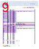




Okay, I've reviewed the provided text which details the pinout of a DDR2 SDRAM chip. Here's a breakdown of the key information and a summary:
Core Function:
The document is a pinout map for a family of DDR2 SDRAM chips. It shows which pins on the chip are used for:
️· Address: Selecting the specific memory location.
️· Data (DQ): The actual data being read or written.
️· Data Strobe (DQS/RDQS/UDQS/LDQS): Signals that time the data.
️· Data Mask (DM/UDM/LDM): Used to enable/disable specific bytes of data.
️· Control Signals: (like clock signals, and read/write enables)
️· Power Supplies (VDD, VDDQ): Providing the necessary voltage for operation.
Key Features & Organization:
️· Multiple Configurations: The chip comes in different configurations: x4, x8, and x16 (referring to the width of the data bus). The pinout varies depending on the configuration.
️· Detailed Pin Descriptions: The table lists each pin, its name, type (Input/Output/Power), and the signal it carries.
️· Signal Types: The document distinguishes between various types of data strobes (DQS, RDQS, UDQS, LDQS) and data masks (DM, UDM, LDM) which provide timing and byte-level control.
️· Power Pins: The pinout clearly identifies the power supply pins (VDD, VDDQ) that are essential for the chip's operation.
Summary:
This document serves as a technical reference for engineers and hardware designers working with DDR2 SDRAM. It provides the necessary information to correctly interface the chip with other components in a system, including how to connect power, data, and control signals. Understanding this pinout is crucial for building reliable and high-performance memory systems using DDR2.
In short, it's a guide to properly connecting and using a DDR2 SDRAM chip.
Is there anything specific you would like me to do with this information? For example:
️· Do you want me to explain a specific pin or signal?
️· Do you want me to compare the pinouts for different configurations (x4, x8, x16)?
️· Do you want me to help you understand how this pinout relates to the overall operation of a memory system?
Core Function:
The document is a pinout map for a family of DDR2 SDRAM chips. It shows which pins on the chip are used for:
️· Address: Selecting the specific memory location.
️· Data (DQ): The actual data being read or written.
️· Data Strobe (DQS/RDQS/UDQS/LDQS): Signals that time the data.
️· Data Mask (DM/UDM/LDM): Used to enable/disable specific bytes of data.
️· Control Signals: (like clock signals, and read/write enables)
️· Power Supplies (VDD, VDDQ): Providing the necessary voltage for operation.
Key Features & Organization:
️· Multiple Configurations: The chip comes in different configurations: x4, x8, and x16 (referring to the width of the data bus). The pinout varies depending on the configuration.
️· Detailed Pin Descriptions: The table lists each pin, its name, type (Input/Output/Power), and the signal it carries.
️· Signal Types: The document distinguishes between various types of data strobes (DQS, RDQS, UDQS, LDQS) and data masks (DM, UDM, LDM) which provide timing and byte-level control.
️· Power Pins: The pinout clearly identifies the power supply pins (VDD, VDDQ) that are essential for the chip's operation.
Summary:
This document serves as a technical reference for engineers and hardware designers working with DDR2 SDRAM. It provides the necessary information to correctly interface the chip with other components in a system, including how to connect power, data, and control signals. Understanding this pinout is crucial for building reliable and high-performance memory systems using DDR2.
In short, it's a guide to properly connecting and using a DDR2 SDRAM chip.
Is there anything specific you would like me to do with this information? For example:
️· Do you want me to explain a specific pin or signal?
️· Do you want me to compare the pinouts for different configurations (x4, x8, x16)?
| Part No. | HYB18T512400B |
| Manufacturer | QIMONDA |
| Size | 3Mb |
| Pages | 68 pages |
| Description | 512-Mbit Double-Data-Rate-Two SDRAM |
| Lei ha avuto il aiuto da alldatasheet? [ DONATE ] |
Di alldatasheet | Richest di pubblicita | contatti | Privacy Policy | Collegamento alla scheda tecnica | scambio Link | Ricerca produttore All Rights Reserved©Alldatasheet.com |
| Russian : Alldatasheetru.com | Korean : Alldatasheet.co.kr | Spanish : Alldatasheet.es | French : Alldatasheet.fr | Italian : Alldatasheetit.com Portuguese : Alldatasheetpt.com | Polish : Alldatasheet.pl | Vietnamese : Alldatasheet.vn Indian : Alldatasheet.in | Mexican : Alldatasheet.com.mx | British : Alldatasheet.co.uk | New Zealand : Alldatasheet.co.nz |
|
Family Site : ic2ic.com |
icmetro.com |
 Italian ▼
  English
 Chinese
 German
 Japanese
 Russian
 Korean
 Spanish
 French
 Portuguese
 Polish
 Vietnamese
 Indian
 Mexican
 British
 New Zealand