|
Motore di ricerca datesheet componenti elettronici |
|
|
Motore di ricerca datesheet componenti elettronici |
|
ISL85415DEMO2Z Scheda tecnica(PDF) 5 Page - Renesas Technology Corp |
|
|
|||||||||||||||||||||||||||||
ISL85415DEMO2Z Scheda tecnica(HTML) 5 Page - Renesas Technology Corp |
|
|
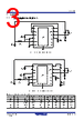
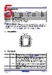
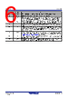
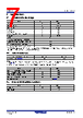
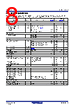
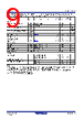
5 / 31 page  ISL85415 1. Overview FN8373 Rev.5.01 Page 5 of 30 Jun.4.20 1.3 Ordering Information 1.4 Pin Configuration 1.5 Pin Descriptions Part Number (Notes 2, 3) Part Marking Temp Range (°C) Tape and Reel (Units) (Note 1) Package (RoHS Compliant) Pkg. Dwg. # ISL85415FRZ 5415 -40 to +125 4.5k 12 Ld DFN L12.4x3 ISL85415FRZ-T 5415 -40 to +125 6k 12 Ld DFN L12.4x3 ISL85415FRZ-T7A 5415 -40 to +125 250 12 Ld DFN L12.4x3 ISL85415EVAL1Z Buck regulator evaluation board ISL85415EVAL2Z Negative buck-boost evaluation board ISL85415DEMO1Z Buck regulator evaluation board (compact version) ISL85415DEMO2Z Dual output isolated buck converter demo board Notes: 1. See TB347 for details about reel specifications. 2. These Pb-free plastic packaged products employ special Pb-free material sets, molding compounds/die attach materials, and 100% matte tin plate plus anneal (e3 termination finish, which is RoHS compliant and compatible with both SnPb and Pb-free soldering operations). Pb-free products are MSL classified at Pb-free peak reflow temperatures that meet or exceed the Pb-free requirements of IPC/JEDEC J STD-020. 3. For Moisture Sensitivity Level (MSL), see the ISL85415 device page. For more information about MSL, see TB363. 12 Ld 4x3 DFN Top View Pin Number Pin Name Description 1 SS The SS pin controls the soft-start ramp time of the output. A single capacitor from the SS pin to ground determines the output ramp rate. See “Soft Start” on page 19 for soft-start details. If the SS pin is tied to VCC, an internal soft-start of 2ms is used. 2 SYNC Synchronization and light load operational mode selection input. Connect to logic high or VCC for PWM mode. Connect to logic low or ground for PFM mode. Logic ground enables the IC to automatically choose PFM or PWM operation. Connect to an external clock source for synchronization with positive edge trigger. Sync source must be higher than the programmed IC frequency. There is an internal 5MΩ pull-down resistor to prevent an undefined logic state if SYNC is left floating. 3 BOOT Floating bootstrap supply pin for the power MOSFET gate driver. The bootstrap capacitor provides the necessary charge to turn on the internal N-Channel MOSFET. Connect an external 100nF capacitor from this pin to PHASE. 4 VIN The input supply for the power stage of the regulator and the source for the internal linear bias regulator. Place a minimum of 4.7µF ceramic capacitance from VIN to GND and close to the IC for decoupling. PIN NUMBER SYMBOL PIN DESCRIPTION |
|
Link URL |
| Lei ha avuto il aiuto da alldatasheet? [ DONATE ] |
Di alldatasheet | Richest di pubblicita | contatti | Privacy Policy | Collegamento alla scheda tecnica | scambio Link | Ricerca produttore All Rights Reserved©Alldatasheet.com |
| Russian : Alldatasheetru.com | Korean : Alldatasheet.co.kr | Spanish : Alldatasheet.es | French : Alldatasheet.fr | Italian : Alldatasheetit.com Portuguese : Alldatasheetpt.com | Polish : Alldatasheet.pl | Vietnamese : Alldatasheet.vn Indian : Alldatasheet.in | Mexican : Alldatasheet.com.mx | British : Alldatasheet.co.uk | New Zealand : Alldatasheet.co.nz |
|
Family Site : ic2ic.com |
icmetro.com |
 Italian ▼
 English
 Chinese
 German
 Japanese
 Russian
 Korean
 Spanish
 French
 Italian
 Portuguese
 Polish
 Vietnamese
 Indian
 Mexican
 British
 New Zealand