|
Motore di ricerca datesheet componenti elettronici |
|
|
Motore di ricerca datesheet componenti elettronici |
|
ISL85415DEMO2Z Scheda tecnica(PDF) 24 Page - Renesas Technology Corp |
|
|
|||||||||||||||||||||||||||||
ISL85415DEMO2Z Scheda tecnica(HTML) 24 Page - Renesas Technology Corp |
|
|
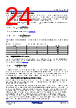
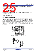
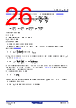
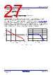
24 / 31 page  ISL85415 7. Application Guidelines FN8373 Rev.5.01 Page 24 of 30 Jun.4.20 7.4 Minimum On/Off-Time Limitation Minimum on-time (tMIN_ON) is the shortest duration of time that the HS FET can be turned on and minimum off- time (tMIN_OFF) is the shortest duration of time that the HS FET can be turned off. The typical tMIN_ON is 90ns and the typical tMIN_OFF is 150ns. For a given tMIN_ON and tMIN_OFF, the higher the switching frequency, the narrower the range of allowed duty cycle, which translates to a smaller range of allowed VIN. For a given output voltage (VOUT) and switching frequency (fsw), the maximum allowed input voltage is given by Equation 5: The minimum allowed voltage is given by Equation 6: Table 2 shows the recommended switching frequencies for the various VOUT to operate up to the maximum VIN of 36V. 7.5 Output Inductor Selection The inductor value determines the converter’s ripple current. Choosing an inductor current requires a somewhat arbitrary choice of ripple current, ΔΙ. A reasonable starting point is 30% of total load current. The inductor value can then be calculated using Equation 7: Increasing the value of inductance reduces the ripple current and threrefore the ripple voltage. However, the larger inductance value can reduce the converter’s response time to a load transient. The inductor current rating should be set so that it does not saturate in overcurrent conditions. For typical ISL85415 applications, inductor values are generally in the 10µH to 47µH range. In general, higher VOUT results in higher inductance. 7.6 Buck Regulator Output Capacitor Selection An output capacitor is required to filter the inductor current. The current mode control loop allows the use of low ESR ceramic capacitors, so it supports very small circuit implementations on the PC board. Electrolytic and polymer capacitors can also be used. While ceramic capacitors offer excellent overall performance and reliability, the actual in-circuit capacitance must be considered. Ceramic capacitors are rated using large peak-to-peak voltage swings and with no DC bias. In the DC/DC converter application, these conditions do not reflect reality. As a result, the actual capacitance can be considerably lower than the advertised value. Consult the manufacturers data sheet to determine the actual in-application capacitance. Most manufacturers publish capacitance vs DC bias so that this effect can be easily accommodated. The effects of AC voltage are not frequently published, but an assumption of ~20% further reduction generally suffices. The result of these considerations can mean an effective capacitance 50% lower than nominal and this value should be used in all design calculations. Nonetheless, ceramic capacitors are a very good choice in many applications due to their reliability and extremely low ESR. Table 2. Recommended Switching Frequencies for Various VOUT VIN (Maximum) (V) VOUT (V) fSW (kHz) 36 5 500 36 3.3 500 36 2.5 500 36 1.8 300 (EQ. 5) VIN max VOUT fSW tMIN_ON -------------------------------------- = (EQ. 6) VIN min VOUT 1f – SW tMIN_OFF -------------------------------------------------- = (EQ. 7) L VIN VOUT – fSW I ------------------------------ VOUT VIN --------------- = |
|
Link URL |
| Lei ha avuto il aiuto da alldatasheet? [ DONATE ] |
Di alldatasheet | Richest di pubblicita | contatti | Privacy Policy | Collegamento alla scheda tecnica | scambio Link | Ricerca produttore All Rights Reserved©Alldatasheet.com |
| Russian : Alldatasheetru.com | Korean : Alldatasheet.co.kr | Spanish : Alldatasheet.es | French : Alldatasheet.fr | Italian : Alldatasheetit.com Portuguese : Alldatasheetpt.com | Polish : Alldatasheet.pl | Vietnamese : Alldatasheet.vn Indian : Alldatasheet.in | Mexican : Alldatasheet.com.mx | British : Alldatasheet.co.uk | New Zealand : Alldatasheet.co.nz |
|
Family Site : ic2ic.com |
icmetro.com |
 Italian ▼
 English
 Chinese
 German
 Japanese
 Russian
 Korean
 Spanish
 French
 Italian
 Portuguese
 Polish
 Vietnamese
 Indian
 Mexican
 British
 New Zealand