|
Motore di ricerca datesheet componenti elettronici |
|
|
Motore di ricerca datesheet componenti elettronici |
|
ISL85415DEMO2Z Scheda tecnica(PDF) 6 Page - Renesas Technology Corp |
|
|
|||||||||||||||||||||||||||||
ISL85415DEMO2Z Scheda tecnica(HTML) 6 Page - Renesas Technology Corp |
|
|
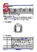
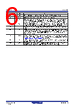
6 / 31 page  ISL85415 1. Overview FN8373 Rev.5.01 Page 6 of 30 Jun.4.20 5 PHASE Switch node output. It connects the switching FET’s with the external output inductor. 6 PGND Power ground connection. Connect directly to the system GND plane. 7 EN Regulator enable input. The regulator and bias LDO are held off when the pin is pulled to ground. When the voltage on this pin rises above 1V, the chip is enabled. Connect this pin to VIN for automatic start-up. Do NOT connect EN pin to VCC since the LDO is controlled by EN voltage. 8 PG Open-drain power-good output that is pulled to ground when the output voltage is below regulation limits or during the soft-start interval. There is an internal 5MΩ internal pull-up resistor. 9 VCC Output of the internal 5V linear bias regulator. Decouple to PGND with a 1µF ceramic capacitor at the pin. 10 FB Feedback pin for the regulator. FB is the inverting input to the voltage loop error amplifier. COMP is the output of the error amplifier. The output voltage is set by an external resistor divider connected to FB. In addition, the PWM regulator’s power-good and UVLO circuits use FB to monitor the regulator output voltage. 11 COMP COMP is the output of the error amplifier. When it is tied to VCC, internal compensation is used. When only an RC network is connected from COMP to GND, external compensation is used. See “Loop Compensation Design” on page 25 for more details. 12 FS Frequency selection pin. Tie to VCC for 500kHz switching frequency. Connect a resistor to GND for adjustable frequency from 300kHz to 2MHz. EPAD GND Signal ground connections. Connect to application board GND plane with at least five vias. All voltage levels are measured with respect to this pin. The EPAD MUST NOT float. Pin Number Pin Name Description |
|
Link URL |
| Lei ha avuto il aiuto da alldatasheet? [ DONATE ] |
Di alldatasheet | Richest di pubblicita | contatti | Privacy Policy | Collegamento alla scheda tecnica | scambio Link | Ricerca produttore All Rights Reserved©Alldatasheet.com |
| Russian : Alldatasheetru.com | Korean : Alldatasheet.co.kr | Spanish : Alldatasheet.es | French : Alldatasheet.fr | Italian : Alldatasheetit.com Portuguese : Alldatasheetpt.com | Polish : Alldatasheet.pl | Vietnamese : Alldatasheet.vn Indian : Alldatasheet.in | Mexican : Alldatasheet.com.mx | British : Alldatasheet.co.uk | New Zealand : Alldatasheet.co.nz |
|
Family Site : ic2ic.com |
icmetro.com |
 Italian ▼
 English
 Chinese
 German
 Japanese
 Russian
 Korean
 Spanish
 French
 Italian
 Portuguese
 Polish
 Vietnamese
 Indian
 Mexican
 British
 New Zealand