|
Motore di ricerca datesheet componenti elettronici |
|
|
Motore di ricerca datesheet componenti elettronici |
|
ADMV1455BBCZ-R7 Scheda tecnica(PDF) 10 Page - Analog Devices |
|
|
|||||||||||||||||||||||||||||
ADMV1455BBCZ-R7 Scheda tecnica(HTML) 10 Page - Analog Devices |
|
|
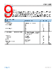
10 / 141 page  Data Sheet ADMV1455 SPECIFICATIONS analog.com Rev. 0 | 10 of 141 TIMING SPECIFICATIONS See the Timing Diagrams Overview section, the Power-Up and Apply the Digital Inputs section, the Initialization SPI Instructions section, the Chip Enable and Operation section, the Chip Disable and Reset section, and the Chip Disable and Power-Down section for additional information. Table 8. Timing Specifications Parameter Min Typ Max Unit Test Conditions/Comments t1 1 100 ms Power supplies 10% to 90% rise time. t2 10 ns Power supplies 90% level to valid digital input time (tDIGITAL). Do not set any logic input levels high prior to tDIGITAL. The RST and CS can go high together after t2 has transpired. If CHIP_ADD0 and CHIP_ADD1 are to be set externally, then set them to the desired logic levels after t2 and prior to any SPI instructions. t3 10 ns RST rising edge to CS falling edge (first SPI instruction after reset). Waiting t3 ensures that the digital logic has reset to the default values. t4 5 ns CS falling edge to SCLK rising edge setup time. t5 10 ns SCLK cycle time (write). t5 20 ns SCLK cycle time (read). t6 2.5 ns SCLK high time. t7 2.5 ns SCLK low time. t8 3 ns SDI data setup time. t9 2 ns SDI data hold time. t10 5 ns SCLK rising edge to CS hold time. t11 5 ns Minimum CS high time for latching in data (for multiple SPI transactions). t12 5 ns CS rising edge to next SCLK rising edge ignore. t13 4 ns SCLK falling edge to SDO valid (load capacitance (CL) = 10pF). t14 5 ns SDO rise and fall time (CL = 10pF). t15 4 ns CS rising edge to SDO tristate (CL = 10pF). t16 10 ns Time from final initialization SPI instruction to entering the operational time (tOPERATIONAL). Set CEN to logic high at this time. t17 5 ns CS rising edge to LOAD pin first rising edge time for loading filter contents. t18 10 ns LOAD pin high time for loading the filter and DSA contents. t19 10 ns LOAD pin low time for preparing to load the DSA offsets. t20 10 ns LOAD pin high time for loading the DSA offsets. t21 0 ns CS falling edge to LOAD pin falling edge time. Both can be set low at the same time after a load operation has been completed (after t18 or t20) and another SPI instruction is desired. t22 10 ns Time from the last SPI instruction when the chip is operational (tCONTINUE)) to the disable time (tDISABLE). After t22 has transpired, set CEN to logic low to disable the chip. t23 3 μs CEN falling edge to RST falling edge. Waiting t23 ensures that the RF portions of the chip have been allowed to power down prior to chip reset. t24 10 ns RST low time to perform reset. t25 3 μs CEN falling edge to the power-down time (tPOWER-DOWN). Waiting t25 ensures that the RF portions of the chip have been allowed to power down prior to shutting down the chip power. t26 10 μs Logic inputs fall time. The logic inputs and power supplies can be turned off at the same time. t27 1 100 ms Power supplies 90% to 10% fall time. |
|
Link URL |
| Lei ha avuto il aiuto da alldatasheet? [ DONATE ] |
Di alldatasheet | Richest di pubblicita | contatti | Privacy Policy | Collegamento alla scheda tecnica | scambio Link | Ricerca produttore All Rights Reserved©Alldatasheet.com |
| Russian : Alldatasheetru.com | Korean : Alldatasheet.co.kr | Spanish : Alldatasheet.es | French : Alldatasheet.fr | Italian : Alldatasheetit.com Portuguese : Alldatasheetpt.com | Polish : Alldatasheet.pl | Vietnamese : Alldatasheet.vn Indian : Alldatasheet.in | Mexican : Alldatasheet.com.mx | British : Alldatasheet.co.uk | New Zealand : Alldatasheet.co.nz |
|
Family Site : ic2ic.com |
icmetro.com |
 Italian ▼
 English
 Chinese
 German
 Japanese
 Russian
 Korean
 Spanish
 French
 Italian
 Portuguese
 Polish
 Vietnamese
 Indian
 Mexican
 British
 New Zealand