|
Motore di ricerca datesheet componenti elettronici |
|
|
Motore di ricerca datesheet componenti elettronici |
|
7480 Scheda tecnica(PDF) 100 Page - Renesas Technology Corp |
|
|
|||||||||||||||||||||||||||||
7480 Scheda tecnica(HTML) 100 Page - Renesas Technology Corp |
|
|
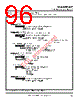
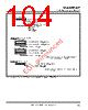
100 / 337 page  7480 Group and 7481 Group User's Manual 1-83 1.12 Timer X and Timer Y HARDWARE Figure 1.12.20 Setting of Programmable Waveform Generation Mode (2) Notes 5: When bit 5 of timer mode register is ‘1’, timer count does not start at this time. Trigger (input signal of INT pin) occurs, at the same time, timer count starts. Notes 6: Keep the trigger width input to INT pin 250 ns or more. Timer X count value is set Procedure 4 Setting timer (Note 4) Timer X low-order (TXL) [Address 00F016] • when timer X is used Timer X high-order (TXH) [Address 00F116] Timer Y count value is set Timer Y low-order (TYL) [Address 00F216] • when timer Y is used Timer Y high-order (TYH) [Address 00F316] Notes 4: When writing to timer, set the low-order byte and high-order byte in this order. Timer XY control register (TXYCON) [Address 00F816] b7 b0 00 Timer X count start (when timer X is used) Timer Y count start (when timer Y is used) Procedure 5 Start of timer count (Note 5) Programmable waveform generation mode (Note 3) Timer Y write control 0: Writing to latch and timer simultaneously 1: Writing to only latch Timer Y mode register (TYM) [Address 00F716] b7 b0 • when timer Y is used Timer Y count source selection 00: f(XIN)/2 01: f(XIN)/8 10: f(XIN)/16 11: Not available 0 0 1 Output level latch Timer Y trigger selection 0: Timer Y free run 1: Trigger occurrence (input signal of INT1 pin) and timer Y start |
|
Link URL |
| Lei ha avuto il aiuto da alldatasheet? [ DONATE ] |
Di alldatasheet | Richest di pubblicita | contatti | Privacy Policy | Collegamento alla scheda tecnica | scambio Link | Ricerca produttore All Rights Reserved©Alldatasheet.com |
| Russian : Alldatasheetru.com | Korean : Alldatasheet.co.kr | Spanish : Alldatasheet.es | French : Alldatasheet.fr | Italian : Alldatasheetit.com Portuguese : Alldatasheetpt.com | Polish : Alldatasheet.pl | Vietnamese : Alldatasheet.vn Indian : Alldatasheet.in | Mexican : Alldatasheet.com.mx | British : Alldatasheet.co.uk | New Zealand : Alldatasheet.co.nz |
|
Family Site : ic2ic.com |
icmetro.com |
 Italian ▼
 English
 Chinese
 German
 Japanese
 Russian
 Korean
 Spanish
 French
 Italian
 Portuguese
 Polish
 Vietnamese
 Indian
 Mexican
 British
 New Zealand