|
Motore di ricerca datesheet componenti elettronici |
|
|
Motore di ricerca datesheet componenti elettronici |
|
F4MP Scheda tecnica(PDF) 7 Page - NXP Semiconductors |
|
|
|||||||||||||||||||||||||||||
F4MP Scheda tecnica(HTML) 7 Page - NXP Semiconductors |
|
|
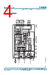
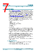
7 / 37 page  PTN3355 All information provided in this document is subject to legal disclaimers. © NXP Semiconductors N.V. 2016. All rights reserved. Product data sheet Rev. 3.1 — 4 November 2016 7 of 37 NXP Semiconductors PTN3355 Low power DP to VGA adapter with integrated 1 : 2 VGA switch 7. Functional description Referring to Figure 1 “Functional diagram”, the PTN3355 performs protocol conversion from VESA DisplayPort specification to VESA VGA output. At the physical layer, PTN3355 implements the advanced DisplayPort Front-end technology (Auto receive equalization, Clock Data Recovery) to support the objectives of delivering excellent Signal Integrity (SI) performance, and consuming very low power consumption. The PTN3355 integrates a DisplayPort receiver (according to VESA DisplayPort standard, Ref. 1) and a high-speed triple 8-bit video digital-to-analog converter that supports a wide range of video resolutions (see Table 9 “Display resolution and pixel clock rate[1]”), up to a pixel clock rate of 240 MHz. The PTN3355 supports one or two DisplayPort Main Link lanes operating at either in 2.7 Gbit/s or 1.62 Gbit/s per lane. PTN3355 also integrates a 1 : 2 VGA switch that enables driving VGA signals either to main board connector or docking connector. This feature helps realize BOM saving due to removal of discrete VGA switch component. PTN3355 comprises the following functional blocks: • DP Main Link • DP AUX CH (Auxiliary Channel) • DPCD (DisplayPort Configuration Data) • VGA monitor detection • Video DAC • 1 : 2 VGA switch The RGB video data with corresponding synchronization references are extracted from the main stream video data. Main stream video attribute information is also extracted. This information is inserted once per video frame during the vertical blanking period by the DP source. The attributes describe the main video stream format in terms of geometry, timing, and color format. The original video clock and video stream are derived from these main link data. The PTN3355 internal DPCD registers can be accessed by the DP source via the DP AUX channel. The monitor’s DDC control bus may also be controlled via the DP AUX channel. PTN3355 implements the standard DisplayPort I2C-over-AUX protocol conversion to provide DP source access to the VGA plug DDC-I2C interface. The PTN3355 passes through sink-side status change (for example, hot-plug events) to the source side, through HPD interrupts and DPCD registers. PTN3355 integrates a 1 : 2 VGA switch that selects between the two channels, depending on DOCK_IN setting. 7.1 DisplayPort Main Link The DisplayPort main link consists of two AC-coupled differential pairs. The 50 termination resistors are integrated inside PTN3355. The PTN3355 supports HBR at 2.7 Gbit/s and RBR at 1.62 Gbit/s per lane. |
|
Link URL |
| Lei ha avuto il aiuto da alldatasheet? [ DONATE ] |
Di alldatasheet | Richest di pubblicita | contatti | Privacy Policy | Collegamento alla scheda tecnica | scambio Link | Ricerca produttore All Rights Reserved©Alldatasheet.com |
| Russian : Alldatasheetru.com | Korean : Alldatasheet.co.kr | Spanish : Alldatasheet.es | French : Alldatasheet.fr | Italian : Alldatasheetit.com Portuguese : Alldatasheetpt.com | Polish : Alldatasheet.pl | Vietnamese : Alldatasheet.vn Indian : Alldatasheet.in | Mexican : Alldatasheet.com.mx | British : Alldatasheet.co.uk | New Zealand : Alldatasheet.co.nz |
|
Family Site : ic2ic.com |
icmetro.com |
 Italian ▼
 English
 Chinese
 German
 Japanese
 Russian
 Korean
 Spanish
 French
 Italian
 Portuguese
 Polish
 Vietnamese
 Indian
 Mexican
 British
 New Zealand