|
Motore di ricerca datesheet componenti elettronici |
|
|
Motore di ricerca datesheet componenti elettronici |
|
ISL73847SEHDEMO2Z Scheda tecnica(PDF) 28 Page - Renesas Technology Corp |
|
|
|||||||||||||||||||||||||||||
ISL73847SEHDEMO2Z Scheda tecnica(HTML) 28 Page - Renesas Technology Corp |
|
|
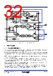
28 / 40 page  R34DS0017EU0104 Rev.1.04 Page 28 Jan 31, 2025 ISL73041SEH Datasheet 6.10 Bootstrap Voltage Overcharge Protection Traditional MOSFET applications drive the gate-source voltage anywhere from 10V-15V while retaining both 1) Low drain-source ON-resistance and 2) reliable operation. GaN FET operation has a much narrower range, usually around 4.5V to 6V, to maintain low ON-resistance and reliable operation. The ISL73041SEH provides an integrated PVCC LDO to provide bias to the low-side gate driver. The ISL73041SEH also features unique circuitry to prevent overcharging the boot voltage in the bootstrap configuration. Unlike a MOSFET, there is no body-drain diode in a GaN FET. However, there is still a reverse conduction path from source to drain with zero gate bias. The source-drain voltage is a function of the reverse current and is provided in the GaN FET datasheet as the VSD parameter. During dead time, when both high and low-side GaN FETs are off, the positive current flowing through the inductor is commutated through the low-side FET source-drain channel. The reverse VSD voltage pulls the PHS node of the ISL73041SEH driver below ground. In traditional half-bridge drivers with a boot diode implementation, the boot diode is forward-biased, and the bootstrap capacitor is charged to PVCC + VSD. Depending on the magnitude, this can over-charge the bootstrap capacitor voltage, which provides the upper gate drive voltage. Important: Operating the GaN FET with higher than recommended gate voltages is unreliable as this can damage the GaN FET. The recommended operating gate voltage for Renesas GaN FETs is 4.5V. The ISL73041SEH implements bootstrap capacitor overcharge protection by replacing an external boot diode with an internal intelligent boot switch. The boot switch turns on only when PWM = 0V and the PHS voltage is within ±250mV of PGND. This avoids recharging the bootstrap capacitor during dead time, where the PHS voltage can be excessively negative such that it overcharges the bootstrap capacitor. Figure 49 and Figure 50 highlight the bootstrap overcharge protection by replacing the boot diode with a boot switch. Figure 49. BOOT Switch Only Figure 50. Schottky BOOT Diode Added UGL PHS LGH LGL IL - Vsd + CBOOT PVCC External Boot Diode Switch Control PWM PHS PVIN I1 I2 BOOT-PHS Voltage Buck Load Current 0A to 15A Transition BOOT-PHS Voltage Buck Load Current 0A to 10A Transition |
|
Link URL |
| Lei ha avuto il aiuto da alldatasheet? [ DONATE ] |
Di alldatasheet | Richest di pubblicita | contatti | Privacy Policy | Collegamento alla scheda tecnica | scambio Link | Ricerca produttore All Rights Reserved©Alldatasheet.com |
| Russian : Alldatasheetru.com | Korean : Alldatasheet.co.kr | Spanish : Alldatasheet.es | French : Alldatasheet.fr | Italian : Alldatasheetit.com Portuguese : Alldatasheetpt.com | Polish : Alldatasheet.pl | Vietnamese : Alldatasheet.vn Indian : Alldatasheet.in | Mexican : Alldatasheet.com.mx | British : Alldatasheet.co.uk | New Zealand : Alldatasheet.co.nz |
|
Family Site : ic2ic.com |
icmetro.com |
 Italian ▼
 English
 Chinese
 German
 Japanese
 Russian
 Korean
 Spanish
 French
 Italian
 Portuguese
 Polish
 Vietnamese
 Indian
 Mexican
 British
 New Zealand