|
Motore di ricerca datesheet componenti elettronici |
|
|
Motore di ricerca datesheet componenti elettronici |
|
ISL73847SEHDEMO2Z Scheda tecnica(PDF) 25 Page - Renesas Technology Corp |
|
|
|||||||||||||||||||||||||||||
ISL73847SEHDEMO2Z Scheda tecnica(HTML) 25 Page - Renesas Technology Corp |
|
|
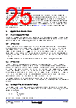
25 / 40 page  R34DS0017EU0104 Rev.1.04 Page 25 Jan 31, 2025 ISL73041SEH Datasheet 5.6 Integrated BOOT Switch The ISL73041SEH integrates a boot switch connected between PVCC and BOOT to charge the bootstrap capacitor. A low rON switch minimizes voltage drop compared to a bootstrap diode while quickly recharging the bootstrap capacitor, which is critical for maintaining the proper Vgs gate drive voltage for the high-side GaN FET. The BOOT switch only turns on when the low-side driver is on, and the phase node voltage is between -250mV and +250mV. The ISL73041SEH internally detects the voltage on the PHS pin (connected to the phase node). The purpose of monitoring the PHS pin voltage and requiring the low-side driver to turn on the boot switch is to prevent over-charging the bootstrap capacitor. See Application Information for more information about boot overcharge protection. 6. Application Information 6.1 Power Supply Biasing ISL73041SEH is biased from the VDD pin and integrates two internal LDOs powered from VDD. The VDD pin bias range is from 4.75V to 18V. A VDD UVLO prevents operation below VDD = 4.75V. Place a 2.2µF or larger ceramic decoupling capacitor near the VDD and SGND pins for input power supply decoupling. 6.2 AVCC LDO The AVCC LDO is for internal chip biasing. AVCC is internally regulated to 5V nominal. AVCC LDO is enabled when VDD is above the UVLO voltage. The AVCC LDO has an internal overcurrent limiting function. When AVCC LDO crosses the overcurrent limit, the AVCC LDO operates in constant current limit regulation. The current capability on AVCC is 20mA, which includes the current internally consumed by the AVCC pin. When AVCC is below the AVCC UVLO threshold, the FLT pin is pulled low to indicate a driver fault condition. Renesas does not recommend using the AVCC LDO for other external biasing; the total current consumption can trigger the constant current limit. It is necessary to place a 1.0µF or larger decoupling capacitor near the AVCC and SGND pins for stability. 6.3 PVCC LDO The PVCC LDO is for the low-side gate drive voltage and the high-side bootstrap circuit. PVCC voltage is externally programmable with a resistor divider to the FB pin. The programmable range is from 4.5V to 5.5V. Optionally, FB can be connected directly to PVCC to set PVCC to 4.5V nominal. The PVCC LDO is enabled by EN pin. The PVCC LDO has an internal overcurrent limiting function. When PVCC LDO crosses the overcurrent limit, the PVCC LDO operates in constant current limit regulation. When PVCC is below the UVLO threshold, the FLT pin is pulled low to indicate a driver fault condition. The current capability on PVCC is 150mA, which includes the current internally consumed by the PVCC pin. Renesas does not recommend using the PVCC LDO for other external biasing; the total current consumption can trigger the constant current limit. It is necessary to place a 1.0µF or larger decoupling capacitor near the PVCC and PGND pins for stability. Renesas recommends using a capacitance on PVCC that is 10x larger than the bootstrap capacitor across BOOT- PHS pins. 6.4 Setting PVCC (Gate Drive) Voltage The voltage on the PVCC LDO to set the gate drive voltage is determined by two resistors connected between PVCC, FB, and SGND. Equation 1 sets the voltage where RF is connected from PVCC to FB and RG is connected between FB and SGND. Optionally, short FB to PVCC to set PVCC = 4.5V. (EQ. 1) PVCC RF RG -------- 1 + 1.2V = |
|
Link URL |
| Lei ha avuto il aiuto da alldatasheet? [ DONATE ] |
Di alldatasheet | Richest di pubblicita | contatti | Privacy Policy | Collegamento alla scheda tecnica | scambio Link | Ricerca produttore All Rights Reserved©Alldatasheet.com |
| Russian : Alldatasheetru.com | Korean : Alldatasheet.co.kr | Spanish : Alldatasheet.es | French : Alldatasheet.fr | Italian : Alldatasheetit.com Portuguese : Alldatasheetpt.com | Polish : Alldatasheet.pl | Vietnamese : Alldatasheet.vn Indian : Alldatasheet.in | Mexican : Alldatasheet.com.mx | British : Alldatasheet.co.uk | New Zealand : Alldatasheet.co.nz |
|
Family Site : ic2ic.com |
icmetro.com |
 Italian ▼
 English
 Chinese
 German
 Japanese
 Russian
 Korean
 Spanish
 French
 Italian
 Portuguese
 Polish
 Vietnamese
 Indian
 Mexican
 British
 New Zealand