|
Motore di ricerca datesheet componenti elettronici |
|
|
Motore di ricerca datesheet componenti elettronici |
|
AD6673 Scheda tecnica(PDF) 37 Page - Analog Devices |
|
|
|||||||||||||||||||||||||||||
AD6673 Scheda tecnica(HTML) 37 Page - Analog Devices |
|
|
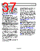
37 / 46 page  AD6673 Data Sheet Rev. C | Page 36 of 45 SERIAL PORT INTERFACE (SPI) The AD6673 SPI allows the user to configure the converter for specific functions or operations through a structured register space provided inside the ADC. The SPI gives the user added flexibility and customization, depending on the application. Addresses are accessed via the serial port and can be written to or read from via the port. Memory is organized into bytes that can be further divided into fields. These fields are documented in the Memory Map section. For detailed operational information, see the AN-877 Application Note, Interfacing to High Speed ADCs via SPI. CONFIGURATION USING THE SPI Three pins define the SPI of this ADC: the SCLK pin, the SDIO pin, and the CS pin (see Table 16). The SCLK (serial clock) pin is used to synchronize the read and write data presented from/to the ADC. The SDIO (serial data input/output) pin is a dual-purpose pin that allows data to be sent and read from the internal ADC memory map registers. The CS (chip select bar) pin is an active low control that enables or disables the read and write cycles. Table 16. Serial Port Interface Pins Pin Function SCLK Serial Clock. The serial shift clock input, which is used to synchronize serial interface, reads and writes. SDIO Serial Data Input/Output. A dual-purpose pin that typically serves as an input or an output, depending on the instruction being sent and the relative position in the timing frame. CS Chip Select Bar. An active low control that gates the read and write cycles. The falling edge of CS, in conjunction with the rising edge of SCLK, determines the start of the framing. An example of the serial timing and its definitions can be found in Figure 56 and Table 5. Other modes involving CS are available. CS can be held low indefinitely, which permanently enables the device; this is called streaming. CS can stall high between bytes to allow for additional external timing. When CS is tied high, SPI functions are placed in a high impedance mode. This mode turns on any SPI pin secondary functions. During an instruction phase, a 16-bit instruction is transmitted. Data follows the instruction phase, and its length is determined by the W0 and the W1 bits. All data is composed of 8-bit words. The first bit of each individual byte of serial data indicates whether a read or write command is issued. This allows the SDIO pin to change direction from an input to an output. In addition to word length, the instruction phase determines whether the serial frame is a read or write operation, allowing the serial port to be used both to program the chip and to read the contents of the on-chip memory. If the instruction is a readback operation, performing a readback causes the SDIO pin to change direction from an input to an output at the appropriate point in the serial frame. Data can be sent in MSB first mode or in LSB first mode. MSB first is the default on power-up and can be changed via the SPI port configuration register. For more information about this and other features, see the AN-877 Application Note, Interfacing to High Speed ADCs via SPI. HARDWARE INTERFACE The pins described in Table 16 comprise the physical interface between the user programming device and the serial port of the AD6673. The SCLK pin and the CS pin function as inputs when using the SPI interface. The SDIO pin is bidirectional, functioning as an input during write phases and as an output during readback. The SPI interface is flexible enough to be controlled by either FPGAs or microcontrollers. One method for SPI configuration is described in detail in the AN-812 Application Note, Microcontroller-Based Serial Port Interface (SPI) Boot Circuit. Do not activate the SPI port during periods when the full dynamic performance of the converter is required. Because the SCLK signal, the CS signal, and the SDIO signal are typically asynchronous to the ADC clock, noise from these signals can degrade converter performance. If the on-board SPI bus is used for other devices, it may be necessary to provide buffers between this bus and the AD6673 to prevent these signals from transitioning at the converter inputs during critical sampling periods. |
|
Link URL |
| Lei ha avuto il aiuto da alldatasheet? [ DONATE ] |
Di alldatasheet | Richest di pubblicita | contatti | Privacy Policy | Collegamento alla scheda tecnica | scambio Link | Ricerca produttore All Rights Reserved©Alldatasheet.com |
| Russian : Alldatasheetru.com | Korean : Alldatasheet.co.kr | Spanish : Alldatasheet.es | French : Alldatasheet.fr | Italian : Alldatasheetit.com Portuguese : Alldatasheetpt.com | Polish : Alldatasheet.pl | Vietnamese : Alldatasheet.vn Indian : Alldatasheet.in | Mexican : Alldatasheet.com.mx | British : Alldatasheet.co.uk | New Zealand : Alldatasheet.co.nz |
|
Family Site : ic2ic.com |
icmetro.com |
 Italian ▼
 English
 Chinese
 German
 Japanese
 Russian
 Korean
 Spanish
 French
 Italian
 Portuguese
 Polish
 Vietnamese
 Indian
 Mexican
 British
 New Zealand