|
Motore di ricerca datesheet componenti elettronici |
|
|
Motore di ricerca datesheet componenti elettronici |
|
AD6673 Scheda tecnica(PDF) 34 Page - Analog Devices |
|
|
|||||||||||||||||||||||||||||
AD6673 Scheda tecnica(HTML) 34 Page - Analog Devices |
|
|
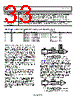
34 / 46 page  Data Sheet AD6673 Rev. C | Page 33 of 45 If there is no far-end receiver termination, or if there is poor differential trace routing, timing errors may result. To avoid such timing errors, it is recommended that the trace length be less than six inches, and that the differential output traces be close together and at equal lengths. Figure 54 shows an example of the digital output (default) data eye and time interval error (TIE) jitter histogram and bathtub curve for the AD6673 lane running at 5 Gbps. Additional SPI options allow the user to further increase the output driver voltage swing of all four outputs to drive longer trace lengths (see Register 0x15 in Table 17). The power dissipation of the DRVDD supply increases when this option is used. See the Memory Map section for more details. The format of the output data is twos complement by default. To change the output data format to offset binary, see the Memory Map section (Register 0x14 in Table 17). ADC OVERRANGE AND GAIN CONTROL In receiver applications, it is desirable to have a mechanism to reliably determine when the converter is about to be clipped. The standard overflow indicator provides delayed information on the state of the analog input that is of limited value in preventing clipping. Therefore, it is helpful to have a programmable threshold below full scale that allows time to reduce the gain before the clip occurs. In addition, because input signals can have significant slew rates, latency of this function is of concern. Using the SPI port, the user can provide a threshold above which the FD output is active. Bit 0 of Register 0x45 enables the fast detect feature. Register 0x47 to Register 0x4B allow the user to set the threshold levels. As long as the signal is below the selected threshold, the FD output remains low. In this mode, the magnitude of the data is considered in the calculation of the condition, but the sign of the data is not considered. The threshold detection responds identically to positive and negative signals outside the desired range (magnitude). ADC OVERRANGE (OR) The ADC overrange indicator is asserted when an overrange is detected on the input of the ADC. The overrange condition is determined at the output of the ADC pipeline and, therefore, is subject to a latency of 36 ADC clock cycles. An overrange at the input is indicated by this bit 36 clock cycles after it occurs. GAIN SWITCHING The AD6673 includes circuitry that is useful in applications either where large dynamic ranges exist, or where gain ranging amplifiers are employed. This circuitry allows digital thresholds to be set such that an upper threshold and a lower threshold can be programmed. One such use is to detect when an ADC is about to reach full scale with a particular input condition. The result is to provide an indicator that can be used to quickly insert an attenuator that prevents ADC overdrive. 0 –0.5 0.5 UIs PERIOD1: HISTOGRAM 6000 7000 –10 0 TIME (ps) 10 5000 4000 1000 0 2000 3000 1–16 1–14 1–12 1–10 1–8 1–6 1–4 1–2 1 3 – 2 – –100 –200 0 100 200 TIME (ps) 400 300 200 100 0 –100 –300 –400 –200 HEIGHT1: EYE DIAGRAM 1 – TJ@BER1: BATHTUB EYE: TRANSITION BITS OFFSET: –0.0072 UIs: 8000; 999992 TOTAL: 8000.999992 0.78 UI Figure 54. AD6673 Digital Outputs Data Eye, Histogram, and Bathtub, External 100 Ω Terminations at 5 Gbps |
|
Link URL |
| Lei ha avuto il aiuto da alldatasheet? [ DONATE ] |
Di alldatasheet | Richest di pubblicita | contatti | Privacy Policy | Collegamento alla scheda tecnica | scambio Link | Ricerca produttore All Rights Reserved©Alldatasheet.com |
| Russian : Alldatasheetru.com | Korean : Alldatasheet.co.kr | Spanish : Alldatasheet.es | French : Alldatasheet.fr | Italian : Alldatasheetit.com Portuguese : Alldatasheetpt.com | Polish : Alldatasheet.pl | Vietnamese : Alldatasheet.vn Indian : Alldatasheet.in | Mexican : Alldatasheet.com.mx | British : Alldatasheet.co.uk | New Zealand : Alldatasheet.co.nz |
|
Family Site : ic2ic.com |
icmetro.com |
 Italian ▼
 English
 Chinese
 German
 Japanese
 Russian
 Korean
 Spanish
 French
 Italian
 Portuguese
 Polish
 Vietnamese
 Indian
 Mexican
 British
 New Zealand