|
Motore di ricerca datesheet componenti elettronici |
|
|
Motore di ricerca datesheet componenti elettronici |
|
AD6673 Scheda tecnica(PDF) 44 Page - Analog Devices |
|
|
|||||||||||||||||||||||||||||
AD6673 Scheda tecnica(HTML) 44 Page - Analog Devices |
|
|
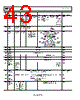
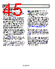
44 / 46 page  Data Sheet AD6673 Rev. C | Page 43 of 45 Reg Addr (Hex) Register Name Bit 7 (MSB) Bit 6 Bit 5 Bit 4 Bit 3 Bit 2 Bit 1 Bit 0 (LSB) Default Notes 0x73 204B parameters, subclass/Np JESD204B subclass; 0x0 = Subclass 0; 0x1 = Subclass 1 (default) JESD204B N’ value; 0xF = N’ = 16 0x2F 0x74 204B parameters, S Reserved; set to 1 JESD204B samples per converter frame cycle (S); read only [Note that this value is in x – 1 format] 0x20 0x75 204B parameters, HD and CF JESD204B HD value; read only JESD204B control words per frame clock cycle per link (CF); read only 0x00 Read Only 0x76 204B RESV1 Reserved Field Number 1 0x00 0x77 204B RESV2 Reserved Field Number 2 0x00 0x78 204B CHKSUM0 JESD204B serial checksum value for Lane 0 0x79 204B CHKSUM1 JESD204B serial checksum value for Lane 1 0x82 204B Lane Assign 1 00 = assign Logical Lane 0 to Physical Lane A [default]; 01 = assign Logical Lane 0 to Physical Lane B Reserved; set to 1 Reserved; set to 0 0x02 0x83 204B Lane Assign 2 Reserved; set to 1 Reserved; set to 1 00 = assign Logical Lane 1 to Physical Lane A; 01 = assign Logical Lane 1 to Physical Lane B (default) 0x31 0x8B 204B LMFC offset Local multiframe clock (LMFC) phase offset value; reset value for LMFC phase counter when SYSREF is asserted; used for deterministic delay applications 0x00 0xA8 204B preemphasis JESD204B preemphasis enable option (consult factory for more detail); set value to 0x04 for preemphasis off; set value to 0x14 for preemphasis on 0x04 Typically not required 0xEE Internal digital clock delay Enable internal clock delay Set to 0 Set to 0 Set to 0 Use incrementing values from 0 to 7 to increase internal digital clock delay; for internal data latching purposes, this does not affect external timing 0x00 See the Synchro- nization section for use 0xEF Internal digital clock delay Enable internal clock delay Set to 0 Set to 0 Set to 0 Use incrementing values from 0 to 7 to increase internal digital clock delay; for internal data latching purposes, this does not affect external timing 0x00 See the Synchro- nization section for use 0xF3 Internal digital clock alignment Force manual realign- ment on Lane 1, self clearing Lane 1 alignment complete Force manual realign- ment on Lane 0, self clearing Lane 0 alignment complete 0x14 See the Synchro- nization section for use 0xFF Device update (global) Transfer settings MEMORY MAP REGISTER DESCRIPTION For more information on functions controlled in Register 0x00 to Register 0x25, see the AN-877 Application Note, Interfacing to High Speed ADCs via SPI. |
|
Link URL |
| Lei ha avuto il aiuto da alldatasheet? [ DONATE ] |
Di alldatasheet | Richest di pubblicita | contatti | Privacy Policy | Collegamento alla scheda tecnica | scambio Link | Ricerca produttore All Rights Reserved©Alldatasheet.com |
| Russian : Alldatasheetru.com | Korean : Alldatasheet.co.kr | Spanish : Alldatasheet.es | French : Alldatasheet.fr | Italian : Alldatasheetit.com Portuguese : Alldatasheetpt.com | Polish : Alldatasheet.pl | Vietnamese : Alldatasheet.vn Indian : Alldatasheet.in | Mexican : Alldatasheet.com.mx | British : Alldatasheet.co.uk | New Zealand : Alldatasheet.co.nz |
|
Family Site : ic2ic.com |
icmetro.com |
 Italian ▼
 English
 Chinese
 German
 Japanese
 Russian
 Korean
 Spanish
 French
 Italian
 Portuguese
 Polish
 Vietnamese
 Indian
 Mexican
 British
 New Zealand