|
Motore di ricerca datesheet componenti elettronici |
|
|
Motore di ricerca datesheet componenti elettronici |
|
AD6673 Scheda tecnica(PDF) 20 Page - Analog Devices |
|
|
|||||||||||||||||||||||||||||
AD6673 Scheda tecnica(HTML) 20 Page - Analog Devices |
|
|
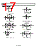
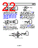
20 / 46 page  Data Sheet AD6673 Rev. C | Page 19 of 45 Input Common Mode The analog inputs of the AD6673 are not internally dc biased. In ac-coupled applications, the user must provide this bias externally. Setting the device so that VCM = 0.5 × AVDD (or 0.9 V) is recommended for optimum performance. An on-board common-mode voltage reference is included in the design and is available from the VCM pin. Using the VCM output to set the input common mode is recommended. Optimum performance is achieved when the common-mode voltage of the analog input is set by the VCM pin voltage (typically 0.5 × AVDD). Decouple the VCM pin to ground by using a 0.1 µF capacitor, as described in the Applications Information section. Place this decoupling capacitor close to the pin to minimize the series resistance and inductance between the part and this capacitor. Differential Input Configurations Optimum performance is achieved while driving the AD6673 in a differential input configuration. For baseband applications, the AD8138, ADA4937-2, ADA4938-2, and ADA4930-2 differential drivers provide excellent performance and a flexible interface to the ADC. The output common-mode voltage of the ADA4930-2 is easily set with the VCM pin of the AD6673 (see Figure 28), and the driver can be configured in a Sallen-Key filter topology to provide band-limiting of the input signal. VIN 76.8 Ω 120 Ω 0.1µF 200 Ω 200 Ω 90 Ω 0.1µF AVDD 33 Ω 33 Ω 33 Ω 15 Ω 15 Ω 5pF 15pF 15pF ADC VIN– VIN+ VCM ADA4930-2 Figure 28. Differential Input Configuration Using the ADA4930-2 For baseband applications where SNR is a key parameter, differential transformer coupling is the recommended input configuration. An example is shown in Figure 29. To bias the analog input, the VCM voltage can be connected to the center tap of the secondary winding of the transformer. 2V p-p 49.9 Ω 0.1µF R1 R1 C1 ADC VIN+ VIN– VCM C2 R2 R3 R2 C2 R3 0.1µF 33 Ω Figure 29. Differential Transformer-Coupled Configuration Consider the signal characteristics when selecting a transformer. Most RF transformers saturate at frequencies below a few megahertz. Excessive signal power can also cause core saturation, which leads to distortion. At input frequencies in the second Nyquist zone and above, the noise performance of most amplifiers is not adequate to achieve the true SNR performance of the AD6673. For applications where SNR is a key parameter, differential double balun coupling is the recommended input configuration (see Figure 30). In this configuration, the input is ac-coupled and the VCM voltage is provided to each input through a 33 Ω resistor. These resistors compensate for losses in the input baluns to provide a 50 Ω impedance to the driver. In the double balun and transformer configurations, the value of the input capacitors and resistors is dependent on the input frequency and source impedance. Based on these parameters, the value of the input resistors and capacitors may need to be adjusted or some components may need to be removed. Table 9 displays recommended values to set the RC network for different input frequency ranges. However, these values are dependent on the input signal and bandwidth and should be used only as a starting guide. Note that the values given in Table 9 are for each R1, R2, C1, C2, and R3 components shown in Figure 29 and Figure 30. Table 9. Example RC Network Frequency Range (MHz) R1 Series (Ω) C1 Differential (pF) R2 Series (Ω) C2 Shunt (pF) R3 Shunt (Ω) 0 to 100 33 8.2 0 15 24.9 100 to 300 15 3.9 0 8.2 24.9 ADC R1 0.1µF 0.1µF 2V p-p VIN+ VIN– VCM C1 C2 R1 R2 R2 0.1µF S 0.1µF C2 33 Ω 33 Ω S P P R3 R3 0.1µF 33 Ω Figure 30. Differential Double Balun Input Configuration |
|
Link URL |
| Lei ha avuto il aiuto da alldatasheet? [ DONATE ] |
Di alldatasheet | Richest di pubblicita | contatti | Privacy Policy | Collegamento alla scheda tecnica | scambio Link | Ricerca produttore All Rights Reserved©Alldatasheet.com |
| Russian : Alldatasheetru.com | Korean : Alldatasheet.co.kr | Spanish : Alldatasheet.es | French : Alldatasheet.fr | Italian : Alldatasheetit.com Portuguese : Alldatasheetpt.com | Polish : Alldatasheet.pl | Vietnamese : Alldatasheet.vn Indian : Alldatasheet.in | Mexican : Alldatasheet.com.mx | British : Alldatasheet.co.uk | New Zealand : Alldatasheet.co.nz |
|
Family Site : ic2ic.com |
icmetro.com |
 Italian ▼
 English
 Chinese
 German
 Japanese
 Russian
 Korean
 Spanish
 French
 Italian
 Portuguese
 Polish
 Vietnamese
 Indian
 Mexican
 British
 New Zealand