|
Motore di ricerca datesheet componenti elettronici |
|
|
Motore di ricerca datesheet componenti elettronici |
|
AD6673 Scheda tecnica(PDF) 19 Page - Analog Devices |
|
|
|||||||||||||||||||||||||||||
AD6673 Scheda tecnica(HTML) 19 Page - Analog Devices |
|
|
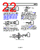
19 / 46 page  AD6673 Data Sheet Rev. C | Page 18 of 45 THEORY OF OPERATION The AD6673 has two analog input channels and two JESD204B output lanes. The signal passes through several stages before appearing at the output port(s). The dual ADC design can be used for diversity reception of signals, where the ADCs operate identically on the same carrier but from two separate antennae. The ADCs can also be operated with independent analog inputs. The user can sample frequencies from dc to 300 MHz using appropriate low-pass or band-pass filtering at the ADC inputs with little loss in ADC performance. Operation to 400 MHz analog input is permitted but occurs at the expense of increased ADC noise and distortion. A synchronization capability is provided to allow synchronized timing between multiple devices. Programming and control of the AD6673 are accomplished using a 3-pin, SPI-compatible serial interface. ADC ARCHITECTURE The AD6673 architecture consists of a dual, front-end, sample- and-hold circuit, followed by a pipelined switched capacitor ADC. The quantized outputs from each stage are combined into a final 11-bit result in the digital correction logic. Alternately, the 11-bit result can be processed through the NSR block before it is sent to the digital correction logic. The pipelined architecture permits the first stage to operate on a new input sample and the remaining stages to operate on the preceding samples. Sampling occurs on the rising edge of the clock. Each stage of the pipeline, excluding the last, consists of a low resolution flash ADC connected to a switched capacitor digital-to- analog converter (DAC) and an interstage residue amplifier (MDAC). The MDAC magnifies the difference between the reconstructed DAC output and the flash input for the next stage in the pipeline. One bit of redundancy is used in each stage to facilitate digital correction of flash errors. The last stage simply consists of a flash ADC. The input stage of each channel contains a differential sampling circuit that can be ac- or dc-coupled in differential or single-ended modes. The output staging block aligns the data, corrects errors, and passes the data to the output buffers. The output buffers are powered from a separate supply, allowing digital output noise to be separated from the analog core. The AD6673 dual IF receiver can simultaneously digitize two channels, making it ideal for diversity reception and digital predistortion (DPD) observation paths in telecommunication systems. The dual IF receiver design can be used for diversity reception of signals, whereas the ADCs operate identically on the same carrier but from two separate antennae. The ADCs can also be operated with independent analog inputs. The user can input frequencies from dc to 300 MHz using appropriate low- pass or band-pass filtering at the ADC inputs with little loss in performance. Operation to a 400 MHz analog input is permitted; however, it occurs at the expense of increased ADC noise and distortion. A synchronization capability is provided to allow synchronized timing between multiple devices. Programming and control of the AD6673 are accomplished using a 3-wire SPI-compatible serial interface. ANALOG INPUT CONSIDERATIONS The analog input to the AD6673 is a differential, switched capacitor circuit that has been designed for optimum performance while processing a differential input signal. The clock signal alternatively switches the input between sample mode and hold mode (see the configuration shown in Figure 27). When the input is switched into sample mode, the signal source must be capable of charging the sampling capacitors and settling within 1/2 clock cycle. A small resistor in series with each input can help reduce the peak transient current that is required from the output stage of the driving source. A shunt capacitor can be placed across the inputs to provide dynamic charging currents. This passive network creates a low-pass filter at the ADC input; therefore, the precise values are dependent on the application. In intermediate frequency (IF) undersampling applications, reduce the shunt capacitors. In combination with the driving source impedance, the shunt capacitors limit the input bandwidth. Refer to the AN-742 Application Note, Frequency Domain Response of Switched-Capacitor ADCs; the AN-827 Application Note, A Resonant Approach to Interfacing Amplifiers to Switched- Capacitor ADCs; and the Analog Dialogue article, “Transformer- Coupled Front-End for Wideband A/D Converters,” for more information on this subject. CPAR1 CPAR1 CPAR2 CPAR2 S S S S S S CFB CFB CS CS BIAS BIAS VIN+ H VIN– Figure 27. Switched-Capacitor Input For best dynamic performance, match the source impedances driving VIN+ and VIN− and differentially balance the inputs. |
|
Link URL |
| Lei ha avuto il aiuto da alldatasheet? [ DONATE ] |
Di alldatasheet | Richest di pubblicita | contatti | Privacy Policy | Collegamento alla scheda tecnica | scambio Link | Ricerca produttore All Rights Reserved©Alldatasheet.com |
| Russian : Alldatasheetru.com | Korean : Alldatasheet.co.kr | Spanish : Alldatasheet.es | French : Alldatasheet.fr | Italian : Alldatasheetit.com Portuguese : Alldatasheetpt.com | Polish : Alldatasheet.pl | Vietnamese : Alldatasheet.vn Indian : Alldatasheet.in | Mexican : Alldatasheet.com.mx | British : Alldatasheet.co.uk | New Zealand : Alldatasheet.co.nz |
|
Family Site : ic2ic.com |
icmetro.com |
 Italian ▼
 English
 Chinese
 German
 Japanese
 Russian
 Korean
 Spanish
 French
 Italian
 Portuguese
 Polish
 Vietnamese
 Indian
 Mexican
 British
 New Zealand