|
Motore di ricerca datesheet componenti elettronici |
|
|
Motore di ricerca datesheet componenti elettronici |
|
AD6673 Scheda tecnica(PDF) 10 Page - Analog Devices |
|
|
|||||||||||||||||||||||||||||
AD6673 Scheda tecnica(HTML) 10 Page - Analog Devices |
|
|
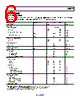
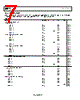
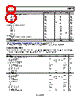
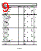
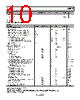
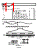
10 / 46 page  Data Sheet AD6673 Rev. C | Page 9 of 45 Parameter Temperature Min Typ Max Unit Low Level Output Voltage (V OL) Full I OL = 1.6 mA Full 0.2 V I OL = 50 µA Full 0.05 V 1 Pull-up. 2 Pull-down. SWITCHING SPECIFICATIONS Table 4. Parameter Symbol Temperature Min Typ Max Unit CLOCK INPUT PARAMETERS Conversion Rate1 f S Full 40 250 MSPS SYSREF± Setup Time to Rising Edge CLK±2 t REFS Full 0.31 ns SYSREF± Hold Time from Rising Edge CLK±2 t REFH Full 0 ns SYSREF± Setup Time to Rising Edge RFCLK2 t REFSRF Full 0.50 ns SYSREF± Hold Time from Rising Edge RFCLK2 t REFHRF Full 0 ns CLK± Pulse Width High t CH Divide-by-1 Mode, DCS Enabled Full 1.8 2.0 2.2 ns Divide-by-1 Mode, DCS Disabled Full 1.9 2.0 2.1 ns Divide-by-2 Mode Through Divide-by-8 Mode Full 0.8 ns Aperture Delay t A Full 1.0 ns Aperture Uncertainty (Jitter) t J Full 0.16 ps rms DATA OUTPUT PARAMETERS Data Output Period or Unit Interval (UI) Full L/(20 × M × f S) Seconds Data Output Duty Cycle 25°C 50 % Data Valid Time 25°C 0.78 UI PLL Lock Time (t LOCK) 25°C 25 µs Wake-Up Time (Standby) 25°C 10 µs Time ADC (Power-Down)3 25°C 250 ms Time Output (Power-Down)4 25°C 50 ms Subclass 0: SYNCINB± Falling Edge to First Valid K.28 Characters (Delay Required for Rx CGS Start) Full 5 Multiframes Subclass 1: SYSREF± Rising Edge to First Valid K.28 Characters (Delay Required for SYNCB± Rising Edge/Rx CGS Start) Full 5 Multiframes CGS Phase K.28 Characters Duration Full 1 Multiframe Pipeline Delay JESD204B M1, L1 Mode (Latency) Full 36 Cycles5 JESD204B M1, L2 Mode (Latency) Full 59 Cycles JESD204B M2, L1 Mode (Latency) Full 25 Cycles JESD204B M2, L2 Mode (Latency) Full 36 Cycles Additional Pipeline Latency with NSR Enabled Full 2 Cycles Fast Detect (Latency) Full 7 Cycles Data Rate per Lane 25°C 5.0 Gbps Uncorrelated Bounded High Probability (UBHP) Jitter 25°C 8 ps Random Jitter at 5.0 Gbps 25°C 1.7 ps rms Output Rise/Fall Time 25°C 60 ps Differential Termination Resistance 25°C 100 Ω Out-of-Range Recovery Time Full 3 Cycles 1 Conversion rate is the clock rate after the divider. 2 Refer to Figure 3 for timing diagram. 3 Wake-up time ADC is defined as the time required for the ADC to return to normal operation from power-down mode. 4 Wake-up time output is defined as the time required for JESD204B output to return to normal operation from power-down mode. 5 Cycles refers to ADC conversion rate cycles. |
|
Link URL |
| Lei ha avuto il aiuto da alldatasheet? [ DONATE ] |
Di alldatasheet | Richest di pubblicita | contatti | Privacy Policy | Collegamento alla scheda tecnica | scambio Link | Ricerca produttore All Rights Reserved©Alldatasheet.com |
| Russian : Alldatasheetru.com | Korean : Alldatasheet.co.kr | Spanish : Alldatasheet.es | French : Alldatasheet.fr | Italian : Alldatasheetit.com Portuguese : Alldatasheetpt.com | Polish : Alldatasheet.pl | Vietnamese : Alldatasheet.vn Indian : Alldatasheet.in | Mexican : Alldatasheet.com.mx | British : Alldatasheet.co.uk | New Zealand : Alldatasheet.co.nz |
|
Family Site : ic2ic.com |
icmetro.com |
 Italian ▼
 English
 Chinese
 German
 Japanese
 Russian
 Korean
 Spanish
 French
 Italian
 Portuguese
 Polish
 Vietnamese
 Indian
 Mexican
 British
 New Zealand